
Voltage Regulator Module (VRM) and Enterprise Voltage Regulator-Down (EVRD) 10.2 Design Guidelines


Voltage Regulator Module (VRM) and Enterprise Voltage 27
Regulator-Down (EVRD) 10.2 Design Guidelines
6 Output Indicators
6.1 Power Good (Vcc_PWRGD - PROPOSED
The VRM/EVRD may provide a power-good output signal, which remains in the low state until a
maximum of 10 ms after the output voltage reaches the range specified in Section 2.2. The signal
should then remain asserted as long as the VRM/EVRD output is operating within specification. It
will be an open-collector/drain or equivalent signal. The pull-up resistor and voltage source will be
located on the baseboard. If this signal is not implemented on the VRM, it should be left
unconnected. Table 6-1shows the Vcc_PWRGD pin specification.
6.2 Voltage Regulator Hot (VR_hot#) - PROPOSED
The VRM/EVRD VR_hot# signal is an output signal that is asserted low when a thermal event is
detected in the converter. Assertion of this signal will be used by the system to minimize damage to
the converter due to the thermal conditions. Table 6-2 shows the VR_hot# pin specification. This
signal will be an open-collector/drain or equivalent signal and needs to be pulled up to an
appropriate voltage through a pull-up resistor on the baseboard. A typical implementation would be
a 50 ohm resistor pulled up to 1.2 V.
Each customer is responsible for identifying maximum temperature specifications for all
components in the VRM/EVRD design and ensuring that these specifications are not violated,
while continuously drawing specified Icc (TDC) levels. In the occurrence of a thermal event, a
thermal sense circuit may assert the processors signal FORCEPR# immediately prior to exceeding
maximum VRM, baseboard, and/or component thermal ratings to prevent heat damage. The
assertion may be made through direct connection to the FORCEPR# pin or through system
management logic. Assertion of this signal will lower processor power consumption and reduce
current draw through the voltage regulator, resulting in lower component temperatures. Sustained
assertion of the FORCEPR# pin will cause noticeable platform performance degradation and
should not occur when drawing less than specified thermal design current for a properly designed
system.
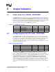
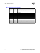
Table 6-1. Vcc_PWRGD Specifications
Symbol Parameter Min Max Units
I
OL
Output Low Current 0 4 mA
V
OH
Output High Voltage 0.8 5.5 V
V
OL
Output Low Voltage 0 0.4 V
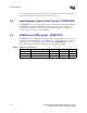
Table 6-2. VR_hot# Specifications
Symbol Parameter Min Max Units
I
OL
Output Low Current 19.9 30 mA
V
OH
Output High Voltage 0.8 3.465 V
V
OL
Output Low Voltage 0 0.4 V