
Voltage Regulator Module (VRM) and Enterprise Voltage Regulator-Down (EVRD) 10.2 Design Guidelines


Voltage Regulator Module (VRM) and Enterprise Voltage 13
Regulator-Down (EVRD) 10.2 Design Guidelines
Output Voltage Requirements
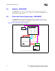
NOTES:
1. V
TT
comes up at the application of system power to the Vtt VR. Vtt is used to supply VID [5:0] power to the
processor.
2. V
TT
VR generates VIDPWRGD after the VTT supply reaches 90% of the final value and must be a minimum
of 1 ms. It is used by the Vcc VR to latch the processor’s core VIDs outputs and should be a qualifier for
enabling the output of the Vcc VR.
3. Vcc_PWRGD is generated by the Vcc VR and may be used elsewhere in the system.
4. VIDPWRGD must deactivate and Vcc must be disabled immediately when Vtt becomes invalid.
5. Vcc should not be enabled until at least 1ms after the VIDPWRGD is asserted.
6. Vcc_PWRGD should assert between 0 and 10 ms after Vcc reaches 90% of the final value.
7. See the processor datasheet for the latest timing requirements.
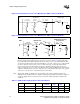
2.6 Dynamic Voltage Identification (D-VID) - REQUIRED
VRM/EVRD 10.2 supports dynamic VID across the entire VID table. The VRM/EVRD must be
capable of accepting voltage level changes of 12.5 mV steps every 5 µs, up to 36 steps (450 mV) in
180 µs. The low voltage state will be maintained for at least 50 µs. The worst case settling time,
including line-to-line skew, for the six VID lines is 400 ns. The VID inputs should contain circuitry
to prevent false tripping or latching of VID codes during the settling time.
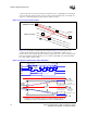
During a transition, the output voltage must be between the maximum voltage of the high range
(“A” in Figure 2-5) and the minimum voltage of the low range (“B”). The VRM/EVRD must
respond to a transition from VID-low to VID-high by regulating its Vcc output to the range defined
by the new, final VID code within 50 µs of the final step. The time to move the output voltage from
VID-high to VID-low will depend on the PWM controller design, the amount of system decoupling
capacitance, and the processor load.
Figure 2-5 shows operating states as a representative processor changes levels. The diagram
assumes steady state, maximum current during the transition for ease of illustration; actual
processor behavior allows for any dIcc/dt event during the transitions, depending on the code it is
executing at that time. In the example, the processor begins in a high-load condition. In transitions
12 and 23, the processor prepares to switch to the low-voltage range with a transition to a low-load
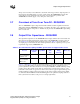
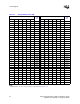
Figure 2-4. Power-On Sequence Timing Diagram
OUTEN
2
5
Vcc
3, 6
Vcc_PWRGD
90% of Vcc
10ms MAX
Stage 2
1
Vtt
VIDPWRGD
2, 4
VID[5:0]
Valid
1
Not-Valid
90%
of Vtt
1ms<t
Vtt
<10ms
Stage 1
1
VIDs are valid as soon as
VIDPWRGD is active