
Voltage Regulator Module (VRM) and Enterprise Voltage Regulator-Down (EVRD) 10.0 Design Guidelines

VRM and EVRD 10.0 Design Guidelines
R
14
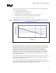
2.5 Stability REQUIRED
The VRM/EVRD needs to be unconditionally stable under all specified output voltage ranges and
current transients of any duty cycle and up to repetition rates of 1 MHz. The VRM/EVRD should
be stable under a no load condition.
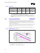
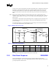
2.6 Processor Power Sequencing REQUIRED
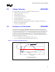
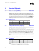
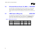
The VRM/EVRD must support platforms with defined power-up sequences. Figure 5 shows a
block diagram of a power sequencing implementation, and Figure 6 shows a timing diagram of
the power sequencing requirements.
Figure 5. Power-On Sequence Block Diagram
Vcc VR
V
TT
Vcc
VIDPWRGD
V
TT
VR
VID [5:0]
Processor
Enable
Vcc_PWRGD
To System
delay*
NOTES: This delay could be built into the V
TT
VR.
Figure 6. Power-On Sequence Timing Diagram
Vcc_PWRGD
Vcc
VID Invalid VID Valid
VIDPWRGD
V
TT
VID[5:0]
1ms min
VID Invalid
0 ms min
10 ms max
10 ms max
NOTES:
1. V
TT
comes up at the application of system power to the V
TT
VR. V
TT
is used to supply power to the VID
logic of the processor.
2. V
TT
VR generates VIDPWRGD, to latch the processor’s VID outputs and enable the Vcc VR, after the
V
TT
supply reaches 90% of the final value.
3. Vcc_PWRGD is generated by the Vcc VR and may be used elsewhere in the system.
4. VIDPWRGD must deactivate and Vcc must be disabled immediately when Vtt becomes invalid.
5. Vcc_PWRGD should assert between 0 and 10 ms after Vcc reaches 90% of the final value.
6. See the Intel® Xeon™ Processor with 800 MHz System Bus Datasheet and Low Voltage Intel® Xeon™
processor with 800 MHz System Bus Datasheet for the latest timing requirements.