
Intel Xeon Processor and Intel E7500/E7501Chipset Compatible Platform Design Guide

Intel
®
Xeon™ Processor and Intel
®
E7500/E7501 Chipset Compatible Platform Design Guide 51
Platform Clock Routing Guidelines
4.1.2 HOST_CLK General Routing Guidelines
• When routing the differential clocks, do not split up the two halves of a differential clock pair
between layers. Route to all agents on the same physical routing layer referenced to ground.
• Do not change routed layers. The goal of constraining all bus clocks to one physical routing
layer is to minimize the impact on skew due to variations in Er and the impedance variations
due to physical tolerances of circuit board material.
• Do not place vias between adjacent complementary clock traces, and avoid differential vias.
Vias placed in one half of a differential pair must be matched by a via in the other half.
Differential vias can be placed within length L1, between clock driver and Rs, if needed to
shorten length L1.
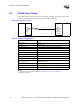
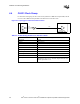
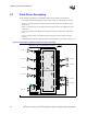
4.1.3 CK408 vs. CK408B Requirement
The CK408 and CK408B are pin compatible. The only difference between the two chips is the
CK408B replaces two signals on the CK408 with a fourth HOST_CLK pair for the In Target Probe
(ITP) and is preferred by board designers for preliminary testing and validation. The CK408
requires pull-up resistors on the additional clock pair while the CK408B pins need to be connected
to the ITP.
• Add one 10 kΩ ± 5% pull-up resistor close to the clock driver before the 33 Ω ± 5% (Rs)
(see Figure 4-5) series resistor on each ITP signal trace (CPU3, CPU3#). This would give the
option to use the CK408 instead of the CK408B.
• When using only a CK408, the 10 kΩ ± 5% pull-up resistor is the only necessary part.
Figure 4-5. Stuffing Options for CK408 and CK408B
CK408: no pop
CK408B: Rs
CK408x
CPU3 / S0
CPU3# /
CPU_STOP#
CK408: 10 kΩ ± 5%
CK408B: no pop
VCC3_3
CK408: no pop
CK408B: Rs
CK408: 10 kΩ ± 5%
CK408B: no pop
VCC3_3
To ITP BCLK1
To ITP BCLK0