
Intel Xeon Processor and Intel E7500/E7501Chipset Compatible Platform Design Guide

Intel
®
Xeon™ Processor and Intel
®
E7500/E7501 Chipset Compatible Platform Design Guide 247
Layout Checklist
14.2 Processor Power Delivery Layout Checklist
All recommendations in this checklist apply to the power distribution design of the processor’s
“VCC_CPU” and ground supply. This checklist assumes the voltage regulator solution adheres to
the guidelines documented in either the
VRM 9.1 DC-DC Converter Design Guidelines or Dual
Intel
®
Xeon™ Processor Voltage Regulator Down (VRD) Design Guidelines depending on which
solution is implemented.
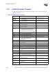
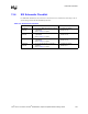
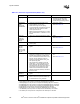
Table 14-2. Processor Power Delivery Layout Checklist (Sheet 1 of 4)
Checklist Items Recommendations Comments
Power / Ground
Plane Copper
Weight
• Use at least 2 oz total copper for the
combined weight of all processor power
planes (VCC_CPU).
• Use at least 2 oz copper for the combined
weight of all processor ground planes.
• These layers can be implemented using two
1 oz copper layers or four ½ oz copper
layers.
• Refer to Section 11.2.2.
Power / Ground
Plane Geometry
• The power / ground supply to both processor
sockets can be distributed as a dedicated
layer of the PCB, a voltage supply plane with
other power islands, or an island on a signal
layer.
• Never distribute processor power with
traces.
• Do not route capacitors to the processor
socket using traces.
• The island or plane connecting the Voltage
Regulator Module (VRM) or Voltage
Regulator Down (VRD) supply to both
processor sockets should not have any
breaks or voids.
• A “trace” is any etch that is less
than the width of the processor
socket.
Power / Ground
Plane Processor
Socket Breakout
• The power / ground planes should
completely surround all of the pins of the
VRM or VRD and processor socket.
• Minimize the size of the processor socket
vias anti-pads where possible. Anti-pads
should be no larger than 35 mils.
• Locations of the capacitor pads on the outer
power layer should not hinder power
distribution by creating a “slot”-shaped
geometry in the plane.
• Avoid vias around the socket breakout area
as much as possible.
• Refer to Section 11.2.2.
• Section 11.2.2 contains an
example of good socket power /
ground plane routing for an inner
layer.
Voltage Regulator Placement and Sense / Feedback Lines
VRM-based
topology
• Use the “Row” pattern topology. • Refer to Section 11.2.4.
VRD-based
topology
• Use the “L” pattern or “Row” pattern
topology.
• Refer to Section 11.2.5.1
VRD sense point • Route the VRD’s voltage sense input signal
to the middle of the VCC_CPU plane. The
location of this plane connection and route is
not critical.
• Refer to Section 11.2.5.3.