
Intel Xeon Processor and Intel E7500/E7501Chipset Compatible Platform Design Guide

Hub Interface
104 Intel
®
Xeon™ Processor and Intel
®
E7500/E7501 Chipset Compatible Platform Design Guide
7.2 Hub Interface 2.0 Implementation
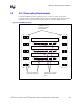
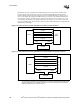
The MCH and P64H2 ballout assignments are optimized to simplify the hub interface routing
between these devices. To allow for greater flexibility in design, a connector can be placed on the
interface to access a HI2.0 agent that resides on an adapter card. The typical card implementation
uses an extension to the 3.3 V PCI-64 connector that provides an additional 70 pins for HI2.0.
Power, JTAG and SMBus signals are taken from the PCI portion of the connector. The remaining
PCI signals are unused. This approach provides the flexibility to allow either a PCI/PCI-X card or a
HI2.0 card to be populated in the slot.
For the 16-bit hub interface, HI[7:0] and HI[20] are associated with PSTRBF and PSTRBS, and
HI[15:8] and HI[21] are associated with PUSTRBF and PUSTRBS. HI[18:16] are common clock
signals; they are sampled using CLK66. The three hub interfaces on the MCH are functionally and
electrically identical. Therefore, these guidelines apply to all three hub interfaces.
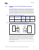
7.2.1 Hub Interface 2.0 High-Speed Routing Guidelines
This section documents the routing guidelines for the Hub Interface 2.0. The Hub Interface 2.0
signal groups are listed in Table 7-2. The general routing guidelines for the Hub Interface 2.0
signals are given in Table 7-3.
NOTE: x = B, C, or D
The hub interface signals must be routed directly from the MCH to P64H2 with all signals
referenced to ground. Maintain a consistent ground reference plane at all times. In addition, route
all signals within a data group (consisting of nine bits of data and a pair of strobes) on the same
layer and reference them to the same ground plane. Keep layer transitions to a minimum. If a layer
change is required, use only two vias per net and keep all signals within a data group on the same
layer.
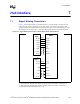
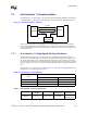
Table 7-1. Hub Interface 2.0 Signal/Strobe Association
Data Group Associated Strobes
HI[7:0]
HI[20]
PSTRBF
PSTRBS
HI[15:8]
HI[21]
PUSTRBF
PUSTRBS
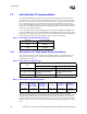
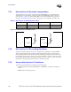
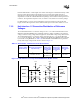
Table 7-2. Hub Interface 2.0 Signal Groups
Group
Signal
MCH Intel
®
P64H2
Common Clock Signals HI[18:16]_x HI[18:16]
Source Synchronous Signals
HI[21:20]_x, HI[15:0]_x,
PSTRBF, PSTRBS, PUSTRBF,
PUSTRBS
HI[21:20],HI[15:0],
PSTRBF, PSTRBS, PUSTRBF,
PUSTRBS
Miscellaneous Signals HIRCOMP_x, HISWNG_x, HIVREF_x HI_RCOMP, HI_VSWING, HI_VREF
Table 7-3. Hub Interface 2.0 Routing Parameters
System Type
Trace Length
Min-Max
(For HI2.0
Device Down)
Trace Length
Min-Max
(For HI2.0 Card
Solution)
Trace Z
0
Trace
Width/Spacing
Breakout
Width/Spacing
533 MHz 3” – 20” 3” – 14” 50 Ω ± 10% 5/15 mils 5/5 mils
(max dist = 0.5”)