
Mobile Intel Pentium 4 Processor Supporting Hyper-Threading Technology on 90-nm Process Technology


54 Mobile Intel® Pentium® 4 Processor Supporting Hyper-Threading Technology on 90-nm Process Technology Datasheet
Pin Listing and Signal Descriptions
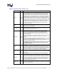
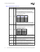
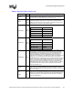
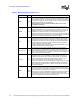
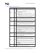
IERR# Output
IERR# (Internal Error) is asserted by a processor as the result of an internal
error. Assertion of IERR# is usually accompanied by a SHUTDOWN transaction
on the processor front side bus. This transaction may optionally be converted to
an external error signal (e.g., NMI) by system core logic. The processor will keep
IERR# asserted until the assertion of RESET#.
This signal does not have on-die termination. Refer to Section 2.4 for
termination requirements.
IGNNE# Input
IGNNE# (Ignore Numeric Error) is asserted to force the processor to ignore a
numeric error and continue to execute noncontrol floating-point instructions. If
IGNNE# is deasserted, the processor generates an exception on a noncontrol
floating-point instruction if a previous floating-point instruction caused an error.
IGNNE# has no effect when the NE bit in control register 0 (CR0) is set.
IGNNE# is an asynchronous signal. However, to ensure recognition of this signal
following an Input/Output write instruction, it must be valid along with the TRDY#
assertion of the corresponding Input/Output Write bus transaction.
INIT# Input
INIT# (Initialization), when asserted, resets integer registers inside the processor
without affecting its internal caches or floating-point registers. The processor
then begins execution at the power-on Reset vector configured during power-on
configuration. The processor continues to handle snoop requests during INIT#
assertion. INIT# is an asynchronous signal and must connect the appropriate
pins of all processor front side bus agents.
If INIT# is sampled active on the active to inactive transition of RESET#, then the
processor executes its Built-in Self-Test (BIST).
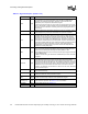
ITP_CLK[1:0] Input
ITP_CLK[1:0] are copies of BCLK that are used only in processor systems
where no debug port is implemented on the system board. ITP_CLK[1:0] are
used as BCLK[1:0] references for a debug port implemented on an interposer. If
a debug port is implemented in the system, ITP_CLK[1:0] are no connects in the
system. These are not processor signals.
LINT[1:0] Input
LINT[1:0] (Local APIC Interrupt) must connect the appropriate pins of all APIC
Bus agents. When the APIC is disabled, the LINT0 signal becomes INTR, a
maskable interrupt request signal, and LINT1 becomes NMI, a nonmaskable
interrupt. INTR and NMI are backward compatible with the signals of those
names on the Pentium processor. Both signals are asynchronous.
Both of these signals must be software configured via BIOS programming of the
APIC register space to be used either as NMI/INTR or LINT[1:0]. Because the
APIC is enabled by default after Reset, operation of these pins as LINT[1:0] is
the default configuration.
LOCK#
Input/
Output
LOCK# indicates to the system that a transaction must occur atomically. This
signal must connect the appropriate pins of all processor front side bus agents.
For a locked sequence of transactions, LOCK# is asserted from the beginning of
the first transaction to the end of the last transaction.
When the priority agent asserts BPRI# to arbitrate for ownership of the processor
front side bus, it will wait until it observes LOCK# deasserted. This enables
symmetric agents to retain ownership of the processor front side bus throughout
the bus locked operation and ensure the atomicity of lock.
Table 4-3. Signal Description (Sheet 5 of 8)
Name Type Description