
Mobile Intel Pentium 4 Processor with 533 MHz Front Side Bus


20 Mobile Intel
®
Pentium
®
4 Processor with 533 MHz System Bus Datasheet
Electrical Specifications
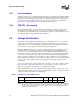
NOTES:
1. Refer to Section 4.2 for signal descriptions.
2. These GTL+ signals do not have on-die termination. Refer to Section 2.5 and the ITP700 Debug Port Design
Guide for termination requirements.
3. In processor systems where there is no debug port implemented on the system board, these signals are used
to support a debug port interposer. In systems with the debug port implemented on the system board, these
signals are no connects.
4. These signal groups are not terminated by the processor. Signals not driven by the ICH4-M component must
be terminated on the system board. Refer to Section 2.5, the ITP700 Debug Port Design Guide, and the
appropriate platform design guidelines listed in Table 1 for termination requirements and further details.
5. The value of these pins during the active-to-inactive edge of RESET# defines the processor configuration
options. See Section 6.1 for details.
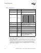
Table 4. FSB Pin Groups
Signal Group Type Signals
1
GTL+ Common Clock Input
Common
clock
BPRI#, DEFER#, RESET#
2
, RS[2:0]#, RSP#, TRDY#
GTL+ Common Clock I/O Synchronous
AP[1:0]#, ADS#, BINIT#, BNR#, BPM[5:0]#
2
, BR0#
2
,
DBSY#, DP[3:0]#, DRDY#, HIT#, HITM#, LOCK#,
MCERR#
GTL+ Source Synchronous
I/O
Source
Synchronous
GTL+ Strobes
Common
Clock
ADSTB[1:0]#, DSTBP[3:0]#, DSTBN[3:0]#
Asynchronous GTL+ Input
4,5
Asynchronous
A20M#, DPSLP#, GHI#, IGNNE#, INIT#
5
, LINT0/INTR,
LINT1/NMI, SMI#
5
, SLP#, STPCLK#
Asynchronous GTL+ Output
4
Asynchronous FERR#/PBE#, IERR#
2
, THERMTRIP#
Asynchronous GTL+ Input/
Output
4
Asynchronous PROCHOT#
TAP Input
4
Synchronous
to TCK
TCK, TDI, TMS, TRST#
TAP Output
4
Synchronous
to TCK
TDO
FSB Clock N/A BCLK[1:0], ITP_CLK[1:0]
3
Power/Other N/A
V
CC
, V
CCA
, V
CCIOPLL
, VCCVID, VID[4:0], V
SS
, V
SSA
,
GTLREF[3:0], COMP[1:0], NC, TESTHI[5:0],
TESTHI[10:8], ITPCLKOUT[1:0], PWRGOOD,
THERMDA, THERMDC, SKTOCC#, V
CC_SENSE
,
V
SS_SENSE,
BSEL[1:0], DBR#
3
Signals Associated Strobe
REQ[4:0]#, A[16:3]#
5
ADSTB0#
A[35:17]#
5
ADSTB1#
D[15:0]#, DBI0# DSTBP0#, DSTBN0#
D[31:16]#, DBI1# DSTBP1#, DSTBN1#
D[47:32]#, DBI2# DSTBP2#, DSTBN2#
D[63:48]#, DBI3# DSTBP3#, DSTBN3#