
Mobile Intel Pentium 4 Processor Supporting Hyper-Threading Technology on 90-nm Process Technology

56 Mobile Intel® Pentium® 4 Processor Supporting Hyper-Threading Technology on 90-nm Process Technology Datasheet
Pin Listing and Signal Descriptions
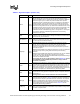
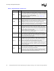
RSP# Input
RSP# (Response Parity) is driven by the response agent (the agent responsible
for completion of the current transaction) during assertion of RS[2:0]#, the
signals for which RSP# provides parity protection. It must connect to the
appropriate pins of all processor front side bus agents.
A correct parity signal is high if an even number of covered signals are low and
low if an odd number of covered signals are low. While RS[2:0]# = 000, RSP# is
also high, since this indicates it is not being driven by any agent guaranteeing
correct parity.
SKTOCC# Output
SKTOCC# (Socket Occupied) will be pulled to ground by the processor. System
board designers may use this pin to determine if the processor is present.
SLP# Input
SLP# (Sleep), when asserted in Stop-Grant state, causes the processor to enter
the Sleep state. During Sleep state, the processor stops providing internal clock
signals to all units, leaving only the Phase-Locked Loop (PLL) still operating.
Processors in this state will not recognize snoops or interrupts. The processor
will recognize only assertion of the RESET# signal, deassertion of SLP# signal,
and assertion of DPSLP# input while in Sleep state. If SLP# is deasserted, the
processor exits Sleep state and returns to Stop-Grant state, restarting its internal
clock signals to the bus and processor core units. If the DPSLP# signal is
asserted while in the Sleep state, the processor will exit the Sleep state and
transition to the Deep Sleep state.
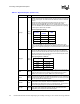
SMI# Input
SMI# (System Management Interrupt) is asserted asynchronously by system
logic. On accepting a System Management Interrupt, the processor saves the
current state and enter System Management Mode (SMM). An SMI
Acknowledge transaction is issued, and the processor begins program execution
from the SMM handler.
If SMI# is asserted during the deassertion of RESET# the processor will tristate
its outputs.
STPCLK# Input
STPCLK# (Stop Clock), when asserted, causes the processor to enter a low
power Stop-Grant state. The processor issues a Stop-Grant Acknowledge
transaction, and stops providing internal clock signals to all processor core units
except the front side bus and APIC units. The processor continues to snoop bus
transactions and service interrupts while in Stop-Grant state. When STPCLK# is
deasserted, the processor restarts its internal clock to all units and resumes
execution. The assertion of STPCLK# has no effect on the bus clock; STPCLK#
is an asynchronous input.
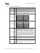
TCK Input
TCK (Test Clock) provides the clock input for the processor Test Bus (also known
as the Test Access Port).
TDI Input
TDI (Test Data In) transfers serial test data into the processor. TDI provides the
serial input needed for JTAG specification support.
TDO Output
TDO (Test Data Out) transfers serial test data out of the processor. TDO
provides the serial output needed for JTAG specification support.
TESTHI[11:0] Input
TESTHI[11:0] must be connected to a V
CC
power source through a resistor for
proper processor operation. See Section 2.4 for more details.
THERMDA Other Thermal Diode Anode. See Section 5.2.7.
THERMDC Other Thermal Diode Cathode. See Section 5.2.7.
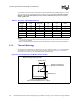
Table 4-3. Signal Description (Sheet 7 of 8)
Name Type Description