
Mobile Intel Pentium 4 Processor Supporting Hyper-Threading Technology on 90-nm Process Technology

Mobile Intel® Pentium® 4 Processor Supporting Hyper-Threading Technology on 90-nm Process Technology Datasheet 53
Pin Listing and Signal Descriptions
DPSLP# Input
DPSLP# when asserted on the platform causes the processor to transition from
the Sleep State to the Deep Sleep state. In order to return to the Sleep State,
DPSLP# must be deasserted and BCLK[1:0] must be running.
DRDY#
Input/
Output
DRDY# (Data Ready) is asserted by the data driver on each data transfer,
indicating valid data on the data bus. In a multi-common clock data transfer,
DRDY# may be deasserted to insert idle clocks. This signal must connect the
appropriate pins of all processor front side bus agents.
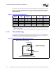
DSTBN[3:0]#
Input/
Output
Data strobe used to latch in D[63:0]#.
DSTBP[3:0]#
Input/
Output
Data strobe used to latch in D[63:0]#.
FERR#/PBE# Output
FERR#/PBE# (floating point error/pending break event) is a multiplexed signal
and its meaning is qualified by STPCLK#. When STPCLK# is not asserted,
FERR#/PBE# indicates a floating-point error and will be asserted when the
processor detects an unmasked floating-point error. When STPCLK# is not
asserted, FERR#/PBE# is similar to the ERROR# signal on the Intel 387
coprocessor, and is included for compatibility with systems using MS-DOS*-type
floating-point error reporting. When STPCLK# is asserted, an assertion of
FERR#/PBE# indicates that the processor has a pending break event waiting for
service. The assertion of FERR#/PBE# indicates that the processor should be
returned to the Normal state. For additional information on the pending break
event functionality, including the identification of support of the feature and
enable/disable information, refer to volume 3 of the Intel Architecture Software
Developer's Manual and the Intel Processor Identification and the CPUID
Instruction application note.
GTLREF Input
GTLREF determines the signal reference level for GTL+ input pins. GTLREF is
used by the GTL+ receivers to determine if a signal is a logical 0 or logical 1.
Refer to the Intel® 852GME and Intel® 852PM Chipset Platforms Design Guide
for more information.
HIT#
HITM#
Input/
Output
Input/
Output
HIT# (Snoop Hit) and HITM# (Hit Modified) convey transaction snoop operation
results. Any front side bus agent may assert both HIT# and HITM# together to
indicate that it requires a snoop stall, which can be continued by reasserting
HIT# and HITM# together.
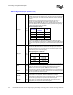
Table 4-3. Signal Description (Sheet 4 of 8)
Name Type Description
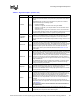
Signals Associated Strobe
D[15:0]#, DBI0# DSTBN0#
D[31:16]#, DBI1# DSTBN1#
D[47:32]#, DBI2# DSTBN2#
D[63:48]#, DBI3# DSTBN3#
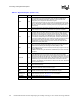
Signals Associated Strobe
D[15:0]#, DBI0# DSTBP0#
D[31:16]#, DBI1# DSTBP1#
D[47:32]#, DBI2# DSTBP2#
D[63:48]#, DBI3# DSTBP3#