
Mobile Intel Pentium 4 Processor Supporting Hyper-Threading Technology on 90-nm Process Technology

16 Mobile Intel® Pentium® 4 Processor Supporting Hyper-Threading Technology on 90-nm Process Technology Datasheet
Electrical Specifications
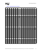
With the implementation of a source synchronous data bus comes the need to specify two sets of
timing parameters. One set is for common clock signals which are dependent upon the rising edge
of BCLK0 (ADS#, HIT#, HITM#, etc.) and the second set is for the source synchronous signals
which are relative to their respective strobe lines (data and address) as well as the rising edge of
BCLK0. Asychronous signals are still present (A20M#, IGNNE#, etc.) and can become active at
any time during the clock cycle. Table 2-3 identifies which signals are common clock, source
synchronous, and asynchronous.
NOTES:
1. Refer to Section 4.2 for signal descriptions.
2. In processor systems where there is no debug port implemented on the system board, these signals are used
to support a debug port interposer. In systems with the debug port implemented on the system board, these
signals are no connects.
3. The value of these pins during the active-to-inactive edge of RESET# defines the processor configuration
options. See Section 6.1 for details.
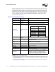
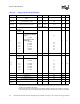
Table 2-3. Front Side Bus Pin Groups
Signal Group Type Signals
1
GTL+ Common Clock
Input
Synchronous to
BCLK[1:0]
BPRI#, DEFER#, RESET#, RS[2:0]#, RSP#, TRDY#
GTL+ Common Clock
I/O
Synchronous to
BCLK[1:0]
AP[1:0]#, ADS#, BINIT#, BNR#, BPM[5:0]#, BR0#, DBSY#,
DP[3:0]#, DRDY#, HIT#, HITM#, LOCK#, MCERR#
GTL+ Source
Synchronous I/O
Synchronous to assoc.
strobe
GTL+ Strobes
Synchronous to
BCLK[1:0]
ADSTB[1:0]#, DSTBP[3:0]#, DSTBN[3:0]#
Asynchronous GTL+
Input
A20M#, DPSLP#, IGNNE#, INIT#, LINT0/INTR, LINT1/NMI,
SMI#, SLP#, STPCLK#
Asynchronous GTL+
Output
FERR#/PBE#, IERR#, THERMTRIP#
Asynchronous GTL+
Input/Output
PROCHOT#
TAP Input Synchronous to TCK TCK, TDI, TMS, TRST#
TAP Output Synchronous to TCK TDO
Front Side Bus Clock Clock BCLK[1:0], ITP_CLK[1:0]
2
Power/Other
V
CC
, VCCA, VCCIOPLL, VID[5:0], VSS, VSSA, GTLREF[3:0],
COMP[1:0], RESERVED, TESTHI[11:0], THERMDA,
THERMDC, VCC_SENSE, VSS_SENSE, VCCVID,
VCCVIDLB, BSEL[1:0], SKTOCC#, DBR#
2
, VIDPWRGD,
BOOTSELECT, OPTIMIZED/COMPAT#
,
PWRGOOD
Signals Associated Strobe
REQ[4:0]#, A[16:3]#
3
ADSTB0#
A[35:17]#
3
ADSTB1#
D[15:0]#, DBI0# DSTBP0#, DSTBN0#
D[31:16]#, DBI1# DSTBP1#, DSTBN1#
D[47:32]#, DBI2# DSTBP2#, DSTBN2#
D[63:48]#, DBI3# DSTBP3#, DSTBN3#