
Mobile Intel Pentium 4 Processor Supporting Hyper-Threading Technology on 90-nm Process Technology

Mobile Intel® Pentium® 4 Processor Supporting Hyper-Threading Technology on 90-nm Process Technology Datasheet 15
Electrical Specifications
2.4 Reserved, Unused, and TESTHI Pins
All RESERVED pins must remain unconnected. Connection of these pins to V
CC
, V
SS
, or to any
other signal (including each other) can result in component malfunction or incompatibility with
future processors. See Chapter 4 for a pin listing of the processor and the location of all
RESERVED pins.
For reliable operation, always connect unused inputs or bidirectional signals to an appropriate
signal level. In a system level design, on-die termination has been included on the processor to
allow signals to be terminated within the processor silicon. Most unused GTL+ inputs should be
left as no connects, as GTL+ termination is provided on the processor silicon. However, see
Table 2-4 for details on GTL+ signals that do not include on-die termination. Unused active high
inputs should be connected through a resistor to ground (V
SS
). Unused outputs can be left
unconnected, however this may interfere with some test access port (TAP) functions, complicate
debug probing, and prevent boundary scan testing. A resistor must be used when tying
bidirectional signals to power or ground. When tying any signal to power or ground, a resistor will
also allow for system testability. For unused GTL+ input or I/O signals, use pull-up resistors of the
same value as the on-die termination resistors (R
TT
).
TAP, Asynchronous GTL+ inputs, and Asynchronous GTL+ outputs do not include on-die
termination. Inputs and used outputs must be terminated on the system board. Unused outputs may
be terminated on the system board or left unconnected. Note that leaving unused outputs
unterminated may interfere with some TAP functions, complicate debug probing, and prevent
boundary scan testing. Signal termination for these signal types is discussed in the Intel
®
852GME
and Intel
®
852PM Chipset Platforms Design Guide.
The TESTHI pins must be tied to the processor V
CC
using a matched resistor, where a matched
resistor has a resistance value within +/-20% of the impedance of the board transmission line
traces. For example, if the trace impedance is 60
Ω, then a value between 48 Ω and 72 Ω is
required.
The TESTHI pins may use individual pull-up resistors or be grouped together as detailed below. A
matched resistor should be used for each group:
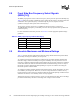
• TESTHI[1:0]
• TESTHI[7:2]
• TESTHI8 - cannot be grouped with other TESTHI signals
• TESTHI9 - cannot be grouped with other TESTHI signals
• TESTHI10 - cannot be grouped with other TESTHI signals
• TESTHI11 - cannot be grouped with other TESTHI signals
2.5 Front Side Bus Signal Groups
The front side bus signals have been combined into groups by buffer type. GTL+ input signals have
differential input buffers, which use GTLREF as a reference level. In this document, the term
"GTL+ Input" refers to the GTL+ input group as well as the GTL+ I/O group when receiving.
Similarly, "GTL+ Output" refers to the GTL+ output group as well as the GTL+ I/O group when
driving.