
Mobile Intel Pentium 4 Processor with 533 MHz Front Side Bus

Mobile Intel
®
Pentium
®
4 Processor with 533 MHz System Bus Datasheet 19
Electrical Specifications
As an alternative, group 2 (TESTHI[5:2]), and the ITPCLKOUT[1:0] pins may be tied directly to
the processor V
CC
. This has no impact on system functionality. TESTHI[0] may also be tied
directly to processor V
CC
if resistor termination is a problem, but matched resistor termination is
recommended. In the case of the ITPCLKOUT[1:0] pins, direct tie to V
CC
is strongly discouraged
for system boards that do not implement an onboard debug port.
Tying any of the TESTHI pins together will prevent the ability to perform boundary scan testing.
Pullup/down resistor requirements for the VID[4:0] and BSEL[1:0] signals are included in the
signal descriptions in Section 4.
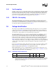
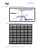
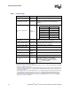
2.6 FSB Signal Groups
In order to simplify the following discussion, the FSB signals have been combined into groups by
buffer type. GTL+ input signals have differential input buffers, which use GTLREF as a reference
level. In this document, the term "GTL+ Input" refers to the GTL+ input group as well as the GTL+
I/O group when receiving. Similarly, "GTL+ Output" refers to the GTL+ output group as well as the
GTL+ I/O group when driving.
With the implementation of a source synchronous data bus comes the need to specify two sets of
timing parameters. One set is for common clock signals that are dependant upon the rising edge of
BCLK0 (ADS#, HIT#, HITM#, etc.) and the second set is for the source synchronous signals
which are relative to their respective strobe lines (data and address) as well as the rising edge of
BCLK0. Asychronous signals are still present (A20M#, IGNNE#, etc.) and can become active at
any time during the clock cycle. Table 4 identifies which signals are common clock, source
synchronous, and asynchronous.