
Mobile Intel Pentium 4 Processor Supporting Hyper-Threading Technology on 90-nm Process Technology

Mobile Intel® Pentium® 4 Processor Supporting Hyper-Threading Technology on 90-nm Process Technology Datasheet 23
Electrical Specifications
3. The loadlines specify voltage limits at the die measured at the V
CC_SENSE
and V
SS_SENSE
pins. Voltage
regulation feedback for voltage regulator circuits must be taken from processor V
CC
and V
SS
pins.
NOTES:
1. Unless otherwise noted, all specifications in this table apply to all processor frequencies.
2. V
IL
is defined as the voltage range at a receiving agent that will be interpreted as a logical low value.
3. V
IH
is defined as the voltage range at a receiving agent that will be interpreted as a logical high value.
4. V
IH
and V
OH
may experience excursions above V
CC
. However, input signal drivers must comply with the signal
quality specifications.
5. Refer to processor I/O Buffer Models for I/V characteristics.
6. The V
CC
referred to in these specifications is the instantaneous V
CC
.
7. Leakage to V
SS
with pin held at V
CC
.
8. Leakage to V
CC
with pin held at 300 mV.
NOTES:
1. Unless otherwise noted, all specifications in this table apply to all processor frequencies.
2. All outputs are open drain.
3. V
IL
is defined as the voltage range at a receiving agent that will be interpreted as a logical low value.
4. V
IH
is defined as the voltage range at a receiving agent that will be interpreted as a logical high value.
5. Refer to the processor I/O Buffer Models for I/V characteristics.
6. The V
CC
referred to in these specifications refers to instantaneous V
CC
.
7. The maximum output current is based on maximum current handling capability of the buffer and is not
specified into the test load.
8. Leakage to Vss with pin held at V
CC
.
9. Leakage to V
CC
with pin held at 300 mV.
10.LINT0/INTR and LINT1/NMI use GTLREF as a reference voltage. For these two signals V
IH
= GTLREF +
(0.10 * V
CC
) and V
IL
= GTLREF - (0.10 * Vcc).
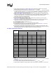
Table 2-10. GTL+ Signal Group DC Specifications
Symbol Parameter Min Max Unit Notes
1
VIL Input Low Voltage 0.0 GTLREF - (0.10 * V
CC
)V2, 6
V
IH Input High Voltage
GTLREF + (0.10 *
V
CC
)
V
CC
V 3, 4, 6
V
OH Output High Voltage 0.90*V
CC
V
CC
V4, 6
I
OL Output Low Current N/A
V
CC
/
[(0.50*R
TT_MIN
)+(R
ON_MIN
)]
A
ILI Input Leakage Current N/A ± 200 µA 7
ILO Output Leakage Current N/A ± 200 µA 8
RON Buffer On Resistance 8 12 Ω 5
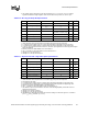
Table 2-11. Asynchronous GTL+ Signal Group DC Specifications
Symbol Parameter Min Max Unit Notes
1
VIL Input Low Voltage 0.0 V
CC
/2 - (0.10 * V
CC
)3, 11
V
IH Input High Voltage V
CC
/2 + (0.10 * V
CC
)V
CC
4, 5, 7,
11
V
OH Output High Voltage 0.90*V
CC
V
CC
V 2, 5, 7
IOL Output Low Current V
CC
/[(0.50*R
TT_MIN
)+(R
ON_MIN
)] A 8
I
LI Input Leakage Current N/A ± 200 µA 9
I
LO
Output Leakage Current N/A ± 200 µA 10
RON Buffer On Resistance 8 12 Ω 6