MIC-3321 3U CompactPCI Pentium M 760 2.
Copyright Notice This document is copyrighted, 2004. All rights are reserved. The original manufacturer reserves the right to make improvements to the products described in this manual at any time without notice. No part of this manual may be reproduced, copied, translated or transmitted in any form or by any means without the prior written permission of the original manufacturer. Information provided in this manual is intended to be accurate and reliable.
Product Warranty Advantech warrants to you, the original purchaser, that each of its products will be free from defects in materials and workmanship for two years from the date of purchase. This warranty does not apply to any products which have been repaired or altered by persons other than repair personnel authorized by Advantech, or which have been subject to misuse, abuse, accident or improper installation. Advantech assumes no liability under the terms of this warranty as a consequence of such events.
Technical Support and Assistance Step 1. Visit the Advantech web site at www.advantech.com/support where you can find the latest information about the product. Step 2. Contact your distributor, sales representative, or Advantech's customer service center for technical support if you need additional assistance.
Contents Chapter 1 Hardware Configuration ................................ 2 1.1 1.2 Introduction ....................................................................... 2 Specifications .................................................................... 3 1.3 Function Block Diagram ................................................... 4 1.4 Board Dimensions ............................................................. 5 1.5 Dip Switch Settings.........................................................
4.2.5 PNP/PCI Configuration Setup ..................................... 29 Figure 4.6:PNP/PCI configuration screen ................... 29 4.2.6 PC Health Status .......................................................... 30 Figure 4.7:PC Health Status setup screen .................... 31 4.2.7 Spread Spectrum Control ............................................ 32 Figure 4.8:PC Health Status setup screen .................... 32 4.2.8 Load Optimized Defaults .............................................
CHAPTER 1 22 Hardware Configuration
Chapter 1 Hardware Configuration 1.1 Introduction MIC-3321 is a 3U, all-in-one, controller board, compliant with PICMG 2.0 R2.1 CompactPCI specifications. For high computing performance, MIC-3321 uses an Intel Pentium M 760 2.0GHz CPU and Intel 915GM chipset. This CPU provides high performance with its on-chip 2 MB L2 cache and is delivered in a Micro-FCBGA 479 package.
1.2 Specifications 1.2.1 Standard SBC Functions • CPU: MIC-3321 supports Intel Pentium M 2.0 GHz • Optional: Celeron M 1.
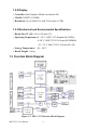
1.2.2 Display • Controller: Intel Graphics Media Accelerator 900 • VRAM: DVMT3.0 128MB • Resolution: Up to 2048x1536 with 32-bit color at 75Hz 1.2.3 Mechanical and Environmental Specifications • Board Size (W x H) : 160 x 100 mm (3U) • Operating Temperature:0 ~ 50° C (MIC-3321 Pentium M 2.0GHz) 0~50° C (MIC-3321LS Celeron M 800MHz) -25 ~ 70° C (MIC-3321C Celeron M 1.0G) • Storage Temperature: -40 ~ 80° C • Board Weight: 0.6 kg 1.3 Function Block Diagram Figure 1.
1.4 Board Dimensions 160 mm 100 mm Figure 1.2: MIC-3321 Board Dimensions 1.5 Dip Switch Settings Since MIC-3321 is composed of one main board and one daughter board, for ease of understanding and a convenient naming, we will use 1F (1st level) to represent the main board, and 2F (2nd level) to represent the daughter board hereafter in this manual. Before setting the switches, you need to disassemble the MIC-3321 to 1F and 2F as in Figures 1.3 and 1.4.
1.5.1 Switch Locations Table 1.1 lists the switch functions of MIC-3321 (be sure that the switch is white one). Figure 1.3 and Figure 1.4 show the locations of S1 and S2, respectively. Table 1.1: MIC-3321 Switch Descriptions DIP-SW Mode Setting Function 1F-S1 Mode Bit-1 : ON LAN1 on Rear I/O Bit-2 : OFF CF : Slave Bit-1 : OFF LAN1 on Front I/O Bit-2 : ON CF : Master 2F-S2 Mode Bit-1 : ON LAN2 on Rear I/O Bit-2 : OFF N/C Bit-1 : OFF LAN2 on Front I/O Bit-2 : ON N/C Figure 1.
Figure 1.4: MIC-3321 S2 Location (2F) 1.6 Safety Precautions Follow these simple precautions to protect yourself and the products. 1. To avoid electrical shock, always disconnect the power from your PC chassis before you work on it. Don't touch any components on the CPU card or other cards while the PC is on. 2. Disconnect power before making any configuration changes. The sudden rush of power as you adjust a switch or install a card may damage sensitive electronic components. 3.
MIC-3321 User Manual 8
CHAPTER 2 22 Connecting Peripherals
Chapter 2 Connecting Peripherals 2.1 Connectors Figure 2.1 and 2.2 show MIC-3321 connector locations. Figure 2.3 shows MIC-3521 connector location. Figure 2.1: MIC-3321 Connector Locations (1F) Figure 2.
Figure 2.
Table 2.1: MIC-3321 Connectors Overview Number Function Description 1F-CN1 USB1 USB1 Type-A Female on Front side panel. 1F-CN3 USB2 USB2 Type-A Female on Front side panel. 1F-CN2 CF CompactFlash socket 1F-CN5 VGA D-Sub 15-pin (Female) on Front side panel. 1F-RJ1 LAN1 10/100/1000Base-TX Ethernet on Front side panel.
2.2 Card Installation The CompactPCI connectors are firm and rigid, but require careful handling while plugging and unplugging. Improper installation of a card can easily damage the backplane of the chassis. The inject/eject handle of MIC-3321 helps you install and remove the card easily and safely. Follow the procedure below to install the MIC3321 into a chassis: To install a card: 1. Hold the card vertically. Be sure that the card is pointing in the correct direction.
To remove a card: 1. Unscrew the four screws on the front panel. 2. Press the lower handle down to release the card from the backplane. 3. Slide the card out. Figure 2.
3 CHAPTER 22 Software Configuration
Chapter 3 Software Configuration 3.1 Overview MIC-3321 has a CD-ROM with utilities and drivers. Please install the Chipset INF driver, VGA graphics driver, and LAN driver. 3.2 Utilities and Drivers The following utilities and drivers are provided with the MIC-3321 series. You can also find updated description of the utilities and drivers in the ReadMe.txt file on the CD-ROM. Windows 2000/XP are fully supported by the MIC-3321 series. 3.2.
4 CHAPTER 22 Award BIOS Setup
Chapter 4 Award BIOS Setup 4.1 Introduction Once you enter the Award BIOS CMOS Setup Utility, the Main Menu (Figure 4-1) will appear on the screen. The Main Menu allows you to select between nine setup functions and two exit choices. Use the arrow keys to select among the items and press to accept or enter the submenu. Figure 4.1: Setup Program Initial Screen Award's BIOS ROM has a built-in Setup program that allows users to modify the basic system configuration.
4.2.1 Standard CMOS Setup Figure 4.2: Standard CMOS Setup Screen. Date The date format is , , , . Time The time format is , based on the 24-hour clock. IDE Primary Master/ Secondary Master/ Secondary Slave IDE HDD Auto-Detection: Press “Enter” to select this option for automatic device detection. IDE Device Setup: Auto: Automatically detects IDE devices during POST None: Select this when no IDE device is used.
Halt On This category determines whether system start-up will halt when an error is detected during power up. The options are: No Errors/All Errors/All, But Keyboard/All, But Diskette/ All, But Disk/Key Memory This category displays base, extended, and total memory detected during the POST (Power On Self Test). 4.2.2 Advanced BIOS Features Setup The "Advanced BIOS FEATURES" screen will appear after the BIOS FEATURES SETUP item from the CMOS SETUP UTILITY Menu was chosen.
Hard Disk Boot Priority Set hard disk boot device priority. CPU Thermal Monitor The Intel Thermal MonitorAutomatic Mode. There are two Automatic modes called Intel Thermal Monitor 1 (TM1) and Intel Thermal Monitor 2 (TM2). And MIC-3321 Auto dete C-M or P-M.When CPU was C-M BIOS running in TM1,another running TM2. TM1: When Intel Thermal Monitor 1 is enabled, and a high temperature situation exists, the clock will be modulated by alternately turning the clock off and on at a 50% duty cycle.
CPU L1 & L2 Cache Enabled (default) Disabled Enable cache Disable cache Note: The internal cache is built into the processor. Quick Power On Self Test This category speeds up Power On Self Test (POST) after you power on the computer. If this is set to Enabled, BIOS will shorten or skip some check items during POST.
Typematic Rate Setting Keystrokes repeat at a rate determined by the keyboard controller. When enabled, the typematic rate and typematic delay can be selected. The settings are: Enabled/Disabled. The default setting is Disabled. Typematic Rate (Chars/Sec) Set the number of times a second to repeat a keystroke key down. The settings are: 6, 8, 10, 12, 15, 20, 24, 30. Typematic Delay (Msec) Sets the delay time after the key is held down before it the keystroke. The settings are: 250, 500, 750, 1000.
4.2.3 Advanced Chipset Features Setup The Advanced Chipset Features Setup option is used to change the values of the chipset registers. These registers control most of the system options in the computer. Choose the "Advanced Chipset Features" from the main menu and the following screen will appear. Figure 4.4: Advanced Chipset Features setup screen DRAM Timing Configuration This field lets you select system memory timing data. Manual and BY SPD are two options.
DRAM RAS# to CAS# Delay This field is used to insert a timing delay between the CAS and RAS strobe signals, used when DRAM is written to, read from, or refreshed. Fast gives faster performance; and Slow gives more stable performance. This field applies only when synchronous DRAM have been installed in the system. The settings are: 2,3,4,5 and auto.
Memory Hole At 15M-16M You can reserve this area of system memory for ISA adapter ROM. When this area is reserved, it cannot be cached. The user information of peripherals that need to use this area of system memory usually discusses their memory requirements. The settings are: Enabled and Disabled (Default). PCI-E Compliancy Mode This allows the user to select the PCI-E compliant mode. The options are [v1.0], and [v1.0a]. On-Chip Video Memory Size This field let you select On-Chip buffer size.
IDE HDD Block Mode Block mode is also called block transfer, multiple commands, or multiple sector read/write. If your IDE hard drive supports block mode (most new drives do), select Enabled for automatic detection of the optimal number of block read/writes per sector the drive can support. The settings are: Enabled (Default), Disabled. On-Chip Primary (SATA) / Secondary (PATA) PCI IDE The integrated peripheral controller contains an IDE interface with support for two IDE channels.
USB Controller Select enabled if your system contains a Universal Serial Bus (USB) 1.1 controller. The settings are: Enabled (Default), Disabled. USB 2.0 Controller Select enabled if your system contains a Universal Serial Bus (USB) 2.0 controller. The settings are: Enabled (Default), Disabled. USB Keyboard Support Select enabled if you use USB Keyboard in DOS mode. Enable (Default) USB Mouse Support Select enabled if you use USB Mouse in DOS mode.
4.2.5 PNP/PCI Configuration Setup This section describes configuring the PCI bus system. PCI, or Personal Computer Interconnect, is a system that allows I/O devices to operate at speeds nearing the speed the CPU itself uses when communicating with its own special components. This section covers some very technical items and it is strongly recommended that only experienced make any changes to the default settings. Figure 4.6: PNP/PCI configuration screen Init Display Fiest The Default is PCI Slot.
Resource Controlled By The Award Plug and Play BIOS has the capacity to automatically configure all the boot and Plug and Play compatible devices. However, this capability means absolutely nothing unless you are using a Plug and Play operating system such as Windows 95/98. If you set this field to "manual," choose specific resources by going into each of the sub menus that follow this field (a sub menu is preceded by a "Y"). The settings are: Auto (ESCD) (Default), Manual.
Figure 4.7: PC Health Status setup screen CPU Warning Temperature This item will prevent the CPU from overheating. The choices are “Disabled”, “50C/122F”, “53C/127F”, “56C/133F”, “60C/140F”, “63C/ 145F”, “66C/151F”, “70C/158F”, “75C/167F”, “80C/176F”, “85C/ 185F”, “90C/194F”, and “95C/205F”. Current System/CPU Temp./ Vcore/1.5V/3.3V/5V/12V/-12V/Vbat This shows system health status.
4.2.7 Spread Spectrum Control Figure 4.8: PC Health Status setup screen Spread Spectrum This allows the enable spread spectrum function. Default is "Dis-abled." 4.2.8 Load Optimized Defaults When you press on this item, you get a confirmation dialog box with a message similar to: Load Optimized Defaults (Y/N) ? N Pressing 'Y' loads the default values that are factory settings for optimal performance system operations.
4.2.9 Set Password To change, confirm, or disable the password, choose the "PASSWORD SETTING" option form the Setup main menu and press [Enter]. The password can be at most 8 characters long. Remember, to enable this feature. You must first select the Security Option in the Advanced BIOS Features Setup to be either "Setup" or "System." Pressing [Enter] again without typing any characters can disable the password setting function.
4.2.10 Save & Exit Setup If you select this and press the [Enter] key, the values entered in the setup utilities will be recorded in the CMOS memory of the chipset. The microprocessor will check this every time you turn your system on and compare this to what it finds as it checks the system. This record is required for the system to operate. 4.2.11 Exit Without Saving Selecting this option and pressing the [Enter] key lets you exit the Setup program without recording any new values or changing old ones.
A APPENDIX 2 Programming the Watchdog Timer
Appendix A Watchdog Timer Programming To program the watchdog timer, you must write a program which writes a value to I/O port address 443 (hex). This output value represents time interval. The value range is from 01 (hex) to FF (hex), and the related time interval is 0.25 sec. to 63.75sec. Data Time Interval 01 0.25 sec. 02 0.50 sec. 03 0.75 sec. 04 1.00 sec. •• •• FF 63.75 sec.
B APPENDIX 2 Pin Assignment
Appendix B Pin Assignment This chapter shows the pin assignments of MIC-3321 series CPU cards. Table B.1: MIC-3321 Connectors Overview Number Function Description 1F-CN1 USB1 USB1 Type-A Female on Front side panel. 1F-CN3 USB2 USB2 Type-A Female on Front side panel. 1F-CN2 CF CompactFlash socket 1F-CN5 VGA D-Sub 15-pin (Female) on Front side panel. 1F-RJ1 LAN1 10/100/1000Base-TX Ethernet on Front side panel.
B.1 CompactFlash Interface The socket accepts an IDE-compatible CompactFlash memory card. Table B.
B.2 USB 2.0 Ports Table B.3: USB 1.1 Ports Pin Definitions Pin Signal 1 VCC 2 USB_P- 3 USB_P+ 4 GND B.
B.4 COM port Table B.4: COM Port Pin Definitions PIN RS-232 1 NDCD 2 NRX 3 NTX 4 NDTR 5 GND 6 NDSR 7 NRTS 8 NCTS 9 NRI B.5 PS/2 Keyboard and Mouse Connector PS/2 keyboard and mouse port pin definitions Table B.
B.6 Ethernet 10/100/1000Base-T RJ-45 Connector Table B.6: Ethernet Connector Definitions Pin Signal 1 TD+ 2 TD- 3 RD+ 4 N/C 5 N/C 6 RD- 7 N/C 8 N/C B.7 Secondary IDE 44-pin 2mm Conn. For direct installation of 2.
Table B.7: Secondary IDE Connectors (2.
B.