
Datasheet


Processor Configuration Registers
218 Datasheet, Volume 2
2.17 Memory Controller MMIO Registers Broadcast
Group
Table 2-19 lists the registers arranged by address offset. Register bit descriptions are in
the sections following the table.
2.17.1 PM_PDWN_Config—Power-down Configuration Register
This register defines the power-down (CKE-off) operation – power-down mode, idle
timer, and global / per rank decision.
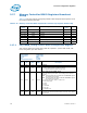
Table 2-19. Memory Controller MMIO Registers Broadcast Group Register Address Map
Address
Offset
Register Symbol Register Name
Reset
Value
Access
0–4CAFh RSVD Reserved — —
4CB0-4CB3h PM_PDWN_config Power-down Configuration 0000_0000h RW-L
4CB4–4CC7h RSVD Reserved — —
4CD0–4F83h RSVD Reserved — —
4F84–4F87h PM_CMD_PWR Power Management Command Power 0000_0000h RW-LV
4F88–4F8Bh PM_BW_LIMIT_config BW Limit Configuration FFFF_03FFh RW-L
4F8C–4F8Fh RSVD Reserved FF1D_1519h RW-L
B/D/F/Type: 0/0/0/MCHBAR_MCBCAST
Address Offset: 4CB0-4CB3h
Default Value: 0000_0000h
Access: RW-L
Size: 32 bits
BIOS Optimal Default: 00000h
Bit Attr
Reset
Value
RST/
PWR
Description
31:13 RO 0h Reserved
12 RW-L 0b Uncore
Global power-down (GLPDN)
1 = Power-down decision is global for channel.
0 = A separate decision is taken for each rank.
11:8 RW-L 0h Uncore
Power-down mode (PDWN_mode)
Selects the mode of power-down. All encodings not in table are
reserved.
Note: When selecting DLL-off or APD-DLL off, DIMM MR0 register
bit 12 (PPD) must equal 0.
Note: When selecting APD, PPD or APD-PPD, DIMM MR0 register
bit 12 (PPD) must equal 1.
The value 0h (no power-down) is a don't care.
0h = No Power Down
1h = APD
2h = PPD
3h = APD-PPD
6h = DLL Off
7h = APD-DLL Off
7:0 RW-L 00h Uncore
Power-down idle timer (PDWN_idle_counter)
This defines the rank idle period in DCLK cycles that causes power-
down entrance.