
Datasheet


Processor Configuration Registers
214 Datasheet, Volume 2
2.16 MCHBAR Registers in Memory Controller –
Common
Table 2-18 lists the registers arranged by address offset. Register bit descriptions are in
the sections following the table.
2.16.1 MAD_CHNL—Address Decoder Channel Configuration
Register
This register defines which channel is assigned to be channel A, channel B, and channel
C according to the rule:
size(A) size (B) size(C)
Since the processor implements only two channels, channel C is always channel 2, and
its size is always 0.
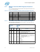
Table 2-18. MCHBAR Registers in Memory Controller – Common Register Address Map
Address
Offset
Register
Symbol
Register Name
Reset
Value
Access
0–4FFFh RSVD Reserved 0h RO
5000–5003h MAD_CHNL Address decoder Channel Configuration 0000_0024h RW-L
5004–5007h MAD_DIMM_ch0 Address Decode Channel 0 0060_0000h RW-L
5008–500Bh MAD_DIMM_ch1 Address Decode Channel 1 0060_0000h RW-L
500C–505Fh RSVD Reserved — —
5060–5063h PM_SREF_config Self Refresh Configuration 0001_00FFh RW-L
5064–50FFh RSVD Reserved — —
B/D/F/Type: 0/0/0/MCHBAR_MCMAIN
Address Offset: 5000–5003h
Reset Value: 0000_0024h
Access: RW-L
Size: 32 bits
BIOS Optimal Default 0000000h
Bit Attr
Reset
Value
RST/
PWR
Description
31:6 RO 0h Reserved
5:4 RW-L 10b Reserved
3:2 RW-L 01b Uncore
Channel B assignment (CH_B)
CH_B defines the mid-size channel:
00 = Channel 0
01 = Channel 1
10 = Channel 2
1:0 RW-L 00b Uncore
Channel A assignment (CH_A)
CH_A defines the largest channel:
00 = Channel 0
01 = Channel 1
10 = Channel 2