
Datasheet


Datasheet, Volume 2 199
Processor Configuration Registers
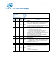
2.12.19 LCAP—Link Capabilities Register
This register indicates DMI specific capabilities.
B/D/F/Type: 0/0/0/DMIBAR
Address Offset: 84–87h
Reset Value: 0001_2C41h
Access: RW-O, RO, RW-OV
Size: 32 bits
BIOS Optimal Default 00002h
Bit Attr
Reset
Value
RST/
PWR
Description
31:18 RO 0h Reserved
17:15 RW-O 010b Uncore
L1 Exit Latency (L1SELAT)
This field indicates the length of time this Port requires to complete
the transition from L1 to L0. The value 010b indicates the range of
2 us to less than 4 us.
000 = Less than 1µs
001 = 1 µs to less than 2 µs
010 = 2 µs to less than 4 µs
011 = 4 µs to less than 8 µs
100 = 8 µs to less than 16 µs
101 = 16 µs to less than 32 µs
110 = 32 µs–64 µs
111 = More than 64 µs
Both bytes of this register that contain a portion of this field must
be written simultaneously in order to prevent an intermediate (and
undesired) value from ever existing.
14:12 RW-O 010b Uncore
L0s Exit Latency (L0SELAT)
This field indicates the length of time this Port requires to complete
the transition from L0s to L0.
000 = Less than 64 ns
001 = 64 ns to less than 128 ns
010 = 128 ns to less than 256 ns
011 = 256 ns to less than 512 ns
100 = 512 ns to less than 1 µs
101 = 1 µs to less than 2 µs
110 = 2 µs–4 µs
111 = More than 4 µs
11:10 RO 11b Uncore
Active State Link PM Support (ASLPMS)
L0s & L1 entry supported.
9:4 RO 04h Uncore
Max Link Width (MLW)
This field indicates the maximum number of lanes supported for
this link.
3:0 RW-OV 0001b Uncore
Max Link Speed (MLS)
This Reset Value reflects gen1.
0001 = 2.5 GT/s Link speed supported
0010 = 5.0 GT/s and 2.5 GT/s Link speeds supported
All other combinations are reserved.