Advanced/RH LPX Motherboard Technical Product Specification Order Number 281809-003 April 1996
THIS SPECIFICATION [DOCUMENT] IS PROVIDED "AS IS" WITH NO WARRANTIES WHATSOEVER, INCLUDING ANY WARRANTY OF MERCHANTABILITY, FITNESS FOR ANY PARTICULAR PURPOSE, OR ANY WARRANTY OTHERWISE ARISING OUT OF ANY PROPOSAL, SPECIFICATION OR SAMPLE. No other license, express or implied, by estoppel or otherwise, to any other intellectual property rights is granted herein.
Advanced/RH Technical Product Specification Table of Contents Introduction MOTHERBOARD MANUFACTURING OPTIONS BOARD LEVEL FEATURES LPX FORM FACTOR CPU PROCESSOR UPGRADE SECOND LEVEL CACHE SYSTEM MEMORY PERIPHERAL COMPONENT INTERCONNECT (PCI) PCISET NATIONAL SEMICONDUCTOR PC87306B SUPER I/O CONTROLLER GRAPHICS SUBSYSTEM AUDIO SUBSYSTEM UNIVERSAL SERIAL BUS (USB) 5 6 7 8 8 9 9 9 10 11 12 13 14 Connectors MOTHERBOARD CONNECTORS FRONT PANEL CONNECTIONS (J3A1, J2A1) AUDIO CONNECTORS BACK PANEL CONNECTORS 14 1
Appendix G − Connectors POWER SUPPLY FRONT PANEL−J3A1 BACK PANEL I/O PERIPHERALS MULTIMEDIA 32 32 33 34 35 36 Appendix-H Motherboard BIOS FLASH MEMORY IMPLEMENTATION BIOS UPGRADES SETUP UTILITY PCI AUTO-CONFIGURATION ISA PLUG ‘N’ PLAY ADVANCED POWER MANAGEMENT LANGUAGE SUPPORT PCI IDE BOOT OPTIONS FLASH LOGO AREA SECURITY FEATURES 39 39 39 40 40 40 40 41 41 41 41 41 Appendix I − PCI Configuration Error Messages 43 Appendix J− − AMIBIOS Error messages and Beep Codes BEEP CODES ERROR MESSAGES ERROR MESS
Introduction The Advanced/RH motherboard integrates the latest advances in processor, memory, and I/O technologies into a standard LPX form factor that provides leading edge technology. This combination of high integration and high performance makes the Advanced/RH motherboard the ideal platform for the increasing requirements of today's (and tomorrow's) desktop applications in the corporate workspace.
MOTHERBOARD MANUFACTURING OPTIONS The following manufacturing options are available. Details for each option are found in the corresponding section of this specification.
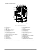
BOARD LEVEL FEATURES A B CD EFG H I J K L M N O P JJ II HH GG FF Q R EE DD S T CC U V BB AA W Z Y X OM04270 Figure 1. Advanced/RH Motherboard Features A − VGA† connector B − Parallel port connector C − COM2 Header D − COM2, or Dual in-line USB Connector E − COM1 connector F− Four Pin CD-ROM audio connector G − PS/2† Mouse port H − PS/2 Keyboard port I − Two 3.
LPX FORM FACTOR The Advanced/RH motherboard is designed to fit into a standard LPX form factor chassis. Figure 2 illustrates the mechanical form factor for the Advanced/RH. The Advanced/RH LPX form factor does adhere to the standard LPX guidelines in that the outer dimensions are 13” x 9”. Location of the I/O connectors, riser slot, and mounting holes are in strict compliance with the LPX specification.
PROCESSOR UPGRADE The Advanced/RH motherboard is manufactured with the 321-pin (socket 7) ZIF processor socket. Socket 7 provides a processor upgrade path that includes higher performance Pentium OverDrive processors than can be supported with socket 5. The motherboard is built to support uniplane CPUs. However, a manufacturing option allows the socket 7 design to support split voltage planes that can supply different voltages for a processor’s CPU core and for the I/O core.
EXPANSION RISER An expansion slot riser connector of EISA form factor provides the capability to support either two or three PCI slots by changing a motherboard jumper to route any extra IRQ and ID selects. A riser board can also support up to five ISA expansion slots. The PCI bus is compliant with the PCI 2.1 specification. To ensure that the lowest positioned slot on the riser card can support a full length add-in card the following conditions must be met.
IDE SUPPORT The Advanced/RH motherboard provides two independent high performance bus-mastering PCI IDE interfaces capable of supporting PIO Mode 3 and Mode 4 devices. The system BIOS supports Cylinder Sector Head (CHS), Logical Block Addressing (LBA) and Extended Cylinder Sector Head (ECHS) translation modes as well as ATAPI (e.g. CD-ROM) devices on both IDE interfaces. IDE device transfer rate and translation mode capability can be automatically determined by the system BIOS.
The integrated 8042 microcontroller contains the AMI Megakey keyboard/mouse controller code which, besides providing traditional keyboard and mouse control functions, supports Power-On/Reset (POR) password protection. The POR password can be defined by the user via the Setup program. The keyboard controller also provides for the following "hot key" sequences: • : System software reset.
ATI-264VT RESOLUTIONS SUPPORTED BY THE MOTHERBOARD Resolution 640x480x4bpp 640x480x8bpp 640x480x16bpp 640x480x24bpp 640x480x32bpp 800x600x4bpp 800x600x8bpp 800x600x16bpp 800x600x24bpp 1024x768x4bpp 1024x768x8bpp 1024x768x16bpp 1280x1024x4bpp 1280x1024x8bpp 1 MB SGRAM X X X X X X X X X X 2 MB SGRAM X X X X X X X X X X X X X X Max Vertical Refresh Rate 100 Hz 100 Hz 100 Hz 100 Hz 60 Hz 100 Hz 100 Hz 100 Hz 100 Hz 100 Hz 100 Hz 100 Hz 75 Hz 75 Hz Table 1.
AUDIO DRIVERS Audio software and utilities are provided for the Advanced/RH motherboard. A Windows setup program installs all of the software programs and utilities onto the system hard drive. Included in the Creative audio software are DOS utilities that allow the user to play a CD-ROM, control sound volume and mixer settings, run diagnostics, and switch between Sound Blaster Pro and Windows Sound System modes.
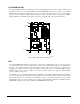
PCI/ISA Expansion Connector(J6J2) CDROM J6N1 1 5 Simm Socket(6) Bank 0(J2D1, J2D2) Bank 1(J2E1, J2F1) Bank 2(J2E1, J2F1) 1 J9N2 4 Modem/Audio Connector 2 1 1 2 Floppy Drive 7 J9K2 J9K1 1 33 J9N1 8 Wave Table 3 PS Remote Connector 34 34 ATI Media Connector (J1H1) 33 1 3.3V Power MIDI Audio J9H1 CELP Connector (J1D1) 6 2 1 1 2 1 J9L1 Primary Power J9H1 PCI IDE Connector(2) J5C1 J6C1 39 40 12 J3A1 29 1 Front Panel I/O Connector OM04275 Figure 3.
POWER SUPPLY CONTROL (J9H1,J9K2) When used with a power supply that supports remote power on/off, the Advanced/RH motherboard can turn off the system power via software control (“soft-off”). The Powerman utility supplied for Windows 3.1x allows for soft-off as does the shutdown icon in Windows 95 Start menu. The system BIOS will turn the system power off when it receives the proper APM command from the OS.
SPEAKER The external speaker provides error beep code information during the Power-On Self Test if the system cannot use the video interface. If no speakers are plugged into the audio output jack, the audio output is redirected to the external PC speaker.
AUDIO CONNECTORS There are two methods of accessing the audio features on the Advanced/RH. The method installed depends on the audio option that has been selected. For business audio, audio is accessed using audio jacks provided on the motherboard. These two 1/8” jacks supply Line Out, and Mic In connections and are available through the back I/O panel. MIDI/AUDIO I/O CONNECTOR Consumer audio is provided by using an audio riser card connected to the audio/midi connector of the motherboard.
WAVE TABLE UPGRADE An eight pin header is provided as part of the consumer audio option to connect to a wave table upgrade card for richer sound quality in both DOS and Windows environments. The wave table upgrade module is simply installed into a standard ISA slot with a cable routed to the connector.
BACK PANEL CONNECTORS The back panel provides external access to PS/2 style keyboard and mouse connectors as well as two serial and one parallel port, which are integrated on the Advanced/RH motherboard. If a USB connector is present, COM2 can be routed to a back panel knockout from the COM2 header on the motherboard. Audio jacks for Speaker Out and Microphone are provided for business audio on the back I/O panel.
Power Consumption Tables 3 and 4 list the measured current and voltage requirements for the Advanced/RH motherboard configured with 16 MB of DRAM. Table 5 lists the typical power consumed by the same configuration.. This information is preliminary and is provided only as a guide for calculating approximate total system power usage with additional resources added. Voltage DC Voltage +3.3V +5V +5V SB (stand by) -5V +12V -12V Acceptable tolerance +/- 5% +/- 5% +/- 5% +/- 5% +/- 5% +/- 5% Table 3.
Appendix A − User-Installable Upgrades SYSTEM MEMORY Supported SIMM Sizes Bank Size Note 512K x 32 (2 MB) 4MB 1 1M x 32 (4 MB) 8MB 2M x 32 (8 MB) 16MB 4M x 32 (16 MB) 32MB 8M x 32 (32 MB) 64MB 2 16M x 32 (64MB) 128MB 2 32M x 32 (128MB) 256MB 2 Table A-1.
HARDWARE MPEG MODULE ATI provides a hardware MPEG module that will work with the Advanced/RH. This module mounts onto connector J1H1, and uses mounting holes provided on the motherboard. This modul is also known as the ATI Multimedia Controller, or AMC. For more information contact ATI Technologies at http://www.atitech.ca, or (905) 882-2626 . . . . . Customer Support (voice) (905) 882-0546 . . . . . Customer Support (fax) (905) 764-9404 . . . . .
Appendix B − Configuration Jumper Settings 3 2 1 6 5 4 D 6 5 4 C 6 5 4 B 6 5 4 A 6 5 4 13.00" 3 2 1 3 2 1 3 2 1 3 2 1 J4L1 J4G1 Clock Speed, CMOS, Password Riser Jumpers 4 5 6 1 2 3 J6C2 OverDrive Voltage Jumper Figure B-1.
FUNCTION FREQ ** (Note: These jumpers also set PCI, and ISA clock speeds.
CPU CONFIGURATION - JUMPER BLOCK J4L1(C&D) These allow the motherboard to be switched between different speeds of the Pentium processor. These jumpers also affect the PCI and ISA clock speeds according to the following table: CPU Freq. (MHz) 166 150 133 120 100 90 75 reserved Host Bus Freq.
DRIVE OR OVERDRIVE - J6C2 Sets the CPU voltage to either standard voltage (3.3v), or OverDrive (3.6v). The Default setting is for a jumper to connect pin 5-6 for standard voltage. Move the jumper to connect pins 4-5 to select OverDrive voltage. RECOVERY JUMPER - J6C2 This jumper should be set to normal mode, Pins 1-2, and should only be moved when a recovery is being performed, i.e. jumper 2-3.
Appendix C − Memory Map Address Range 1024K-512M 960K-1023K Address Range 100000-20000000 F0000-FFFFF Size 511M 64K Description Extended Memory AMI System run time BIOS 944K-959K EC000-EFFFF 16K Main BIOS Recovery Code 936K-943K EA000-EBFFF 8K ESCD (Plug ‘N’ Play configuration area) 928K-935K E8000-E9FFF 8K OEM LOGO (available as UMB) 896K-927K E0000-E7FFF 32K BIOS RESERVED (Currently available as UMB) 800-895K C8000-DFFFF 96K Available HI DOS memory (open to ISA and PCI bus) 640K-79
Appendix D − I/O Map Address (hex) 0000 - 000F 0020 - 0021 Size 16 bytes 2 bytes Description PIIX - DMA 1 PIIX - Interrupt Address (hex) 0388 - 038B 03B4 - 03B5 Size 4 bytes 2 bytes 002E - 002F 2 bytes Ultra I/O configuration 03BA 1 byte 0040 - 0043 4 bytes PIIX - Timer 1 03BC - 03BF 4 bytes 0048 - 004B 4 bytes PIIX - Timer 2 03C0 - 03CA 12 bytes Description Parallel Port 3 0060 1 byte Keyboard Controller 03CC 1 byte 0061 1 byte PIIX - NMI, speaker 03CE - 03CF 2 bytes 0064 1
Appendix E − PCI Configuration Space Map The 82430HX PCIset uses Configuration Mechanism 1 to access PCI configuration space. The PCI Configuration Address register is a 32-bit register located at CF8h, the PCI Configuration Data register is a 32-bit register located at CFCh. These registers are only accessible by full DWORD accesses. The table below lists the PCI bus and device numbers used by the motherboard. Bus Number (h ) 00 00 Dev Number (hex) 00 07 Func.
Appendix F − Interrupts & DMA Channels IRQ System Resource NMI 0 I/O Channel Check Reserved, Interval Timer 1 Reserved, Keyboard buffer full 2 Reserved, Cascade interrupt from slave PIC 3 Serial Port 2 4 Serial Port 1 5 Audio 6 Floppy 7 Parallel Port 1 8 Real Time Clock 9 User available 10 User available 11 Audio 12 Onboard Mouse Port 13 Reserved, Math coprocessor 14 15 Primary IDE Secondary IDE if present, else user available Table F-1.
Appendix G − Connectors POWER SUPPLY PRIMARY POWER J9H1 Pin Name Function 1 2 PWRGD +5 V Power Good + 5 volts Vcc 3 +12 V + 12 volts 4 -12 V - 12 volts 5 GND Ground 6 GND Ground 7 GND Ground 8 GND Ground 9 -5 V -5 volts 10 +5 V + 5 volts Vcc 11 +5 V + 5 volts Vcc 12 +5 V + 5 volts Vcc PCI (3.3V) POWER J9J1 NOT POPULATED Pin Name Function 1 2 GND GND Ground Ground 3 GND Ground 4 +3.3 V + 3.3 volts 5 +3.3V + 3.3 volts 6 +3.3 V + 3.
FRONT PANEL− J3A1 SLEEP/RESUME Pin Signal Name 15 16 SW_ON GND 17 SLEEP 18 SLEEPPU 19 KEY INFRA-RED Pin Signal Name 25 24 CONIRRX IRTX 23 POWER INTERFACE DRIVE LED (DISK) Pin Signal Name GND 14 13 PWRPU PWDRV 22 IRRIN 12 HDA 21 NC 11 HDPU 20 VCC HARD POWER LED / KEYLOCK POWER INTERFACE CPU FAN Signal Name 3 2 Ground +12V 31 Ground POWER INTERFACE SPEAKER CONNECTOR Signal Name 10 9 PWDRV NC 8 PWRPU 7 KEY POWER INTERFACE CONNECTOR Pin Signal Name Pin Signal Name
BACK PANEL I/O PS/2 KEYBOARD J8N1 & MOUSE PORTS J7N1 Pin Signal Name 1 2 Data No Connect 3 Ground 4 Vcc 5 Clock SERIAL PORTS COM1 J6N2 & COM2 J5N1 PARALLEL PORT J3N1 Pin Signal Name 1 2 DCD Serial In - (SIN) Signal Name STROBEData Bit 0 Pin 1 2 Pin 14 15 3 Serial Out - (SOUT) Data Bit 1 3 16 INIT- 4 DTR- Data Bit 2 4 17 SLCT IN- 5 GND Data Bit 3 5 18 Ground 6 DSR- Data Bit 4 6 19 Ground 7 RTS- Data Bit 5 7 20 Ground 8 CTS- Data Bit 6 8 21 Ground 9 RI
PERIPHERALS IDE CONNECTORS J5C1 & J6C1 Signal Name Reset IDE Host Data 7 Pin 1 3 Pin 2 4 Host Data 6 5 6 Host Data 9 Host Data 5 7 8 Host Data 10 Host Data 4 9 10 Host Data 11 Host Data 3 11 12 Signal Name Ground Host Data 8 Host Data 12 Host Data 2 13 14 Host Data 13 Host Data 1 15 16 Host Data 14 Host Data 0 17 18 Host Data 15 Ground 19 20 Key DDRQ0 (DDRQ1) 21 22 Ground I/O Write- 23 24 Ground I/O Read- 25 26 Ground IOCHRDY 27 28 Vcc pull-up DDACK0 (DDAC
MULTIMEDIA MIDI/AUDIO CONNECTOR J9L1 Signal Name +5 V JoyStick But0 Pin 1 3 Pin 2 4 Signal Name +5 V JoyStick But2 JoyStick X1 5 6 JoyStick X2 Ground 7 8 MIDI Out Ground 9 10 JoyStick Y2 JoyStick Y1 11 12 JoyStick But3 JoyStick But1 13 14 MIDI In +5 V 15 16 Key Key 17 18 Key Line Out Right 19 20 Ground Right Speaker 21 22 Ground Left Speaker 23 24 Key Line Out Left 25 26 Ground Line In Right 27 28 -12 V ATI MULTI-MEDIA CON.
PCI / ISA RISER (J6J2) Signal Name Pin Pin Signal Name Signal Name Pin Pin Signal Name IOCHKSD7 A1 A2 B1 B2 GND RSTDRV GND GND E1 E2 F1 F2 GND GND SD6 A3 B3 Vcc PCIINT0- E3 F3 PCIINT2- SD5 A4 B4 IRQ9 PCIINT1- E4 F4 PCIINT3- SD4 A5 B5 -5V Vcc E5 F5 Vcc SD3 A6 B6 DRQ2 Key E6 F6 Key SD2 A7 B7 -12V Vcc E7 F7 Vcc PCLKF SD1 A8 B8 0WS- PCIRST- E8 F8 SD0 A9 B9 +12V GNT0- E9 F9 GND IOCHRDY A10 B10 GND REQ0- E10 F10 GNT1- AEN A11 B11 SM
CELP 2.
Appendix-H Motherboard BIOS The Advanced/RH motherboard uses an Intel BIOS, which is stored in Flash EEPROM and easily upgraded using a floppy disk-based program. BIOS upgrades can be down loaded from the Intel Applications Support electronic bulletin board service, or the Intel FTP site. In addition to the Intel BIOS, the Flash EEPROM also contains the Setup utility, Power-On Self Tests (POST), APM 1.1, the PCI auto-configuration utility, and Windows 95 ready Plug ‘N’ Play.
SETUP UTILITY The ROM-based Setup utility allows the configuration to be modified without opening the system for most basic changes. The Setup utility is accessible only during the Power-On Self Test (POST) by pressing the key after the POST memory test has begun and before boot begins. A prompt may be enabled that informs users to press the key to access Setup. A jumper setting (See table B-1 in appendix B) on the motherboard can be set to prevent user access to Setup for security purposes.
APM is enabled in BIOS by default, however, the system must be configured with an APM driver (such as Power.exe for DOS or vpowerd.386 for Windows 3.x) in order for the system power saving features to take effect. Windows 95 will enable APM automatically upon detecting the presence of the APM BIOS. LANGUAGE SUPPORT The BIOS setup screen and help messages are supported in 32 languages. There are 5 languages translated at this time for use; American English, German, Italian, French, and Spanish.
If the password is forgotten, it can be cleared by turning off the system and setting the "password clear" jumper (See Appendix B: table B-1) to the ON position and briefly powering up the system. The Administrative password and User password are both cleared by this operation. After returning the jumper to the “password keep” position, a new password can be entered in Setup to re-enable password protection.
Appendix I − PCI Configuration Error Messages The following PCI messages are displayed as a group with bus, device and function information.
Appendix J− − AMIBIOS Error messages and Beep Codes Errors can occur during POST (Power On Self Test) which is performed every time the system is powered on. Fatal errors, which prevent the system from continuing the boot process, are communicated through a series of audible beeps. Other errors are displayed in the following format: ERROR Message Line 1 ERROR Message Line 2 For most displayed error messages, there is only one message. If a second message appears, it is "RUN SETUP".
ERROR MESSAGES (CONT.) CMOS Time and Date Not Set Diskette Boot Failure Run Standard CMOS Setup to set the date and time in CMOS RAM. The boot disk in floppy drive A: is corrupt. It cannot be used to boot the system. Use another boot disk and follow the screen instructions. The display jumper is not implemented on this product, this error will not occur. Error in the DMA controller. Error in the first DMA channel. Error in the second DMA channel.
Appendix K − Soft-off Control The Advanced/RH design supports Soft-off control via the SMM code in the BIOS. The CS1 pin out of the National 306B Ultra I/O controller is connected to the Soft-off control line in our power supply circuit. The registers in the Ultra I/O controller that sets the I/O address and control of the CS1 pin is NOT setup until the SMM code is activated.
Appendix L − Environmental Standards MOTHERBOARD SPECIFICATIONS Parameter Temperature Condition Non-Operating Operating Specification -40oC to +70oC +0oC to +55oC (minimum air flow of 200 LFM) DC Voltage +5 V -5 V +12 V -12 V ±5 % ±5 % ±5 % ±5 % Vibration Unpackaged Packaged 5 Hz to 20 Hz : 0.01g² Hz sloping up to 0.02 g² Hz 20 Hz to 500 Hz : 0.02g² Hz (flat) 10 Hz to 40 Hz : 0.015g² Hz (flat) 40 Hz to 500 Hz : 0.015g² Hz sloping down to 0.
Appendix M − Reliability Data The Mean-Time-Between-Failures (MTBF) data is calculated from predicted data @ 55C.