
User's Manual
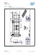
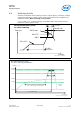
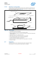
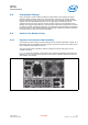
Table Of Contents
- 1.0 General Device Overview
- 2.0 Basic Operating Information
- 3.0 eUniStone Interfaces
- 4.0 General Device Capabilities
- 5.0 Bluetooth Capabilities
- 6.0 Electrical Characteristics
- 7.0 Package Information
- 8.0 Bluetooth Qualification and Regulatory Certification
- 8.1 Reference Design
- 8.2 FCC Class B Digital Devices Regulatory Notice
- 8.3 FCC Wireless Notice
- 8.4 FCC Interference Statement
- 8.5 FCC Identifier
- 8.6 European R&TTE Declaration of Conformity
- 8.7 Bluetooth Qualified Design ID
- 8.8 Industry Canada Certification
- 8.9 Label Design of the Host Product
- 8.10 Regulatory Test House
- 9.0 Assembly Guidelines
- References
- Terminology

eUniStone
PBA 31309
Assembly Guidelines
User’s Manual Intel Public 45
Hardware Description Revision 1.0, 1-Feb-2013
9.9.2 Parameters with an Impact on Voiding
If the void content has to be reduced following parameters have an impact.
Solderability on module and PCB
Bad solderability is often connected to oxidation and has therefore a major impact on
voiding. Flux will get entrapped on oxidized surfaces. In general, Ni/Au pads show
fewer voids than HASL and OSP.
Solder paste
Higher activity of the flux will remove oxide rapidly and less flux will get entrapped.
Voiding increases with increasing solder paste exposure time, since long exposure time
will result in more oxidation and moisture pickup.
Pad size
A large soldering pad means that the outgassing flux has a longer way to the surface of
the solder, and will thereby create more voids.
Solder paste
Smaller powder size and higher metal load means more metal surface to deoxidize and
thereby more entrapped flux and voiding. Higher metal load does also mean higher
viscosity and more difficult for outgassed flux to remove from the solder.
Stencil thickness
A thick solder paste stencil means more surface area to the air and thereby easier for
the outgassing flux to leave the solder.
Temperature soldering profile
Too short preheat time means that the flux does not get enough time to react and flux
get entrapped in the solder and create voids.
Too long reflow time gives larger voids
Too short reflow time gives a fraction of voids