
User's Manual
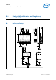


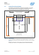
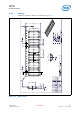
Table Of Contents
- 1.0 General Device Overview
- 2.0 Basic Operating Information
- 3.0 eUniStone Interfaces
- 4.0 General Device Capabilities
- 5.0 Bluetooth Capabilities
- 6.0 Electrical Characteristics
- 7.0 Package Information
- 8.0 Bluetooth Qualification and Regulatory Certification
- 8.1 Reference Design
- 8.2 FCC Class B Digital Devices Regulatory Notice
- 8.3 FCC Wireless Notice
- 8.4 FCC Interference Statement
- 8.5 FCC Identifier
- 8.6 European R&TTE Declaration of Conformity
- 8.7 Bluetooth Qualified Design ID
- 8.8 Industry Canada Certification
- 8.9 Label Design of the Host Product
- 8.10 Regulatory Test House
- 9.0 Assembly Guidelines
- References
- Terminology

eUniStone
PBA 31309
Assembly Guidelines
User’s Manual Intel Public 39
Hardware Description Revision 1.0, 1-Feb-2013
9.3 Solder Paste Printing
The solder paste deposited on the PCB by stencil printing has to be of eutectic or near
eutectic tin leadfree / lead composition. A no-clean solder paste is preferred, since
cleaning of the solder joints is difficult because of the small gap between the module
and the PCB.
Preferred thickness of the solder paste stencil is 100 - 127 µmm (4 - 5 mils). The
apertures on the solder paste stencil shall be of the same size as the pads, 0.6 mm.
9.4 Assembly
9.4.1 Component Placement
In order to assure a high yield, good placement on the PCB is necessary. As a rule of
thumb the tolerable misplacement is 150 µmm. This means that the eUniStone module
can be assembled with a variety of placement systems.
It is recommended to use a vision system capable of package pad recognition and
alignment that evaluates the pad locations on the package (in contrast to outline
centring). This eliminates the pad to package edge tolerance.
The recommendation is to pick and place the module with a nozzle in the centre of the
shield. The nozzle diameter shall not be bigger than 4 mm.
9.4.2 Pin Mark
Pin 1 (A1) is marked on bottom footprint and on the top of the shield on the module
according to Figure 15. Diameter of pin 1 mark on the shield is 0.40 mm.
Figure 15. Pin Marking
i intel
GYYWW/DFYWW9EXX
FCCID:
QG2331308
PBA31309 V1.00
Top_and_Bottom_Views.vsd
Pin 1 marking bottom side
F2F3F4F5F6
E1E2E3E4E5E6E7E8E9
D1D2D3D4D5D6D7D8
C1C2C3C4C5C6C7C8
B1B2B3B4B5B6B7B8B9
A2A3A4A5A6A7A8 A1
F9 F7 F1F8
D9
C9
A9
Pin 1 marking top side
A11
F12 F11
A12