
User's Manual
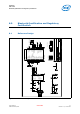


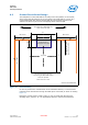
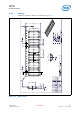
Table Of Contents
- 1.0 General Device Overview
- 2.0 Basic Operating Information
- 3.0 eUniStone Interfaces
- 4.0 General Device Capabilities
- 5.0 Bluetooth Capabilities
- 6.0 Electrical Characteristics
- 7.0 Package Information
- 8.0 Bluetooth Qualification and Regulatory Certification
- 8.1 Reference Design
- 8.2 FCC Class B Digital Devices Regulatory Notice
- 8.3 FCC Wireless Notice
- 8.4 FCC Interference Statement
- 8.5 FCC Identifier
- 8.6 European R&TTE Declaration of Conformity
- 8.7 Bluetooth Qualified Design ID
- 8.8 Industry Canada Certification
- 8.9 Label Design of the Host Product
- 8.10 Regulatory Test House
- 9.0 Assembly Guidelines
- References
- Terminology

eUniStone
PBA 31309
Assembly Guidelines
User’s Manual Intel Public 38
Hardware Description Revision 1.0, 1-Feb-2013
9.2 Printed Circuit Board Design
The land pattern on the PCB shall be according to the land pattern on the module,
which means that the diameter of the LGA pads on the PCB shall be 0.6 mm. It is
recommended that each pad on the PCB shall be surrounded by a solder mask
clearance of about 75 µm to avoid overlapping solder mask and pad.
Figure 14. Cutout Drawing
In order to preserve the characteristics of the embedded antenna, a cutout must be
respected under the antenna through all metal layers of the PCB, as shown in drawing
Figure 14.
Placing the module inside a metal housing or close to metal parts like fasteners,
shielding cages, washers, etc. can significantly affect the antenna characteristics.
Min. 40mm
15.6
3.00
8.7
Min. 15mmMin. 15mm
Visio-Source-PAN1322.vsd
Restricted Area
No copper in any layer
5.00
Dimensions are in mm.
Use a Ground plane in the area
surrounding the PBA31309 module
wherever possible.
If possible place PBA31309in the
center of the main PCB.
Place PBA31309 at the
edge of the main PCB.
Top View