
User's Manual


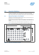
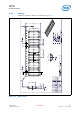
Table Of Contents
- 1.0 General Device Overview
- 2.0 Basic Operating Information
- 3.0 eUniStone Interfaces
- 4.0 General Device Capabilities
- 5.0 Bluetooth Capabilities
- 6.0 Electrical Characteristics
- 7.0 Package Information
- 8.0 Bluetooth Qualification and Regulatory Certification
- 8.1 Reference Design
- 8.2 FCC Class B Digital Devices Regulatory Notice
- 8.3 FCC Wireless Notice
- 8.4 FCC Interference Statement
- 8.5 FCC Identifier
- 8.6 European R&TTE Declaration of Conformity
- 8.7 Bluetooth Qualified Design ID
- 8.8 Industry Canada Certification
- 8.9 Label Design of the Host Product
- 8.10 Regulatory Test House
- 9.0 Assembly Guidelines
- References
- Terminology

eUniStone
PBA 31309
Assembly Guidelines
User’s Manual Intel Public 37
Hardware Description Revision 1.0, 1-Feb-2013
9.0 Assembly Guidelines
The target of this chapter is to provide guidelines for customers to successfully
introduce the eUniStone module in production. This includes general description, PCB-
design, solder printing process, assembly, soldering process, rework and inspection.
9.1 General Description of the Module
eUniStone is a Land Grid Array (LGA 6x12) module made for surface mounting. The
pad diameter is 0.6 mm and the pitch 1.2 mm.
All solder joints on the module will reflow during soldering on the mother board. All
components and shield will stay in place due to wetting force. Wave soldering is not
possible.
Surface treatment on the module pads is Nickel (5-8 µm)/Gold (0.04 - 0.10 µm).
Figure 13 shows the pad layout on the module, seen from the component side.
Figure 13. Pad Layout on the Module (top view)
F2 F3 F4 F5
E1 E2 E3 E4 E5 E6 E7 E8 E9
D1 D2 D3 D4 D5 D6 D7 D8
C1 C2 C3 C4 C5 C6 C7 C8
B1 B2 B3 B4 B5 B6 B7 B8 B9
A2 A3 A4 A5 A6 A7 A8A1
1.0
8.70 mm
0.6
5.0
0. 6
1. 35 1.351.2
F9
1.2
F7F1 F8
D9
C9
A9
15.6 mm
F6 F11
A11
F1 2
A12
2.4