
User's Manual
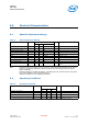
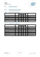
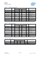
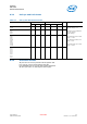
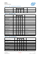
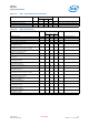
Table Of Contents
- 1.0 General Device Overview
- 2.0 Basic Operating Information
- 3.0 eUniStone Interfaces
- 4.0 General Device Capabilities
- 5.0 Bluetooth Capabilities
- 6.0 Electrical Characteristics
- 7.0 Package Information
- 8.0 Bluetooth Qualification and Regulatory Certification
- 8.1 Reference Design
- 8.2 FCC Class B Digital Devices Regulatory Notice
- 8.3 FCC Wireless Notice
- 8.4 FCC Interference Statement
- 8.5 FCC Identifier
- 8.6 European R&TTE Declaration of Conformity
- 8.7 Bluetooth Qualified Design ID
- 8.8 Industry Canada Certification
- 8.9 Label Design of the Host Product
- 8.10 Regulatory Test House
- 9.0 Assembly Guidelines
- References
- Terminology

eUniStone
PBA 31309
Electrical Characteristics
User’s Manual Intel Public 26
Hardware Description Revision 1.0, 1-Feb-2013
6.3.4 System Power Consumption
Note: I/O currents are not included since they depend mainly on external loads. For more
details see [2].
6.4 RF Part
6.4.1 Characteristics RF Part
The characteristics involve the spread of values to be within the specific temperature
range. Typical characteristics are the median of the production.
All values refers to Intel reference design.
6.4.1.1 Bluetooth Related Specifications
Table 12. Max. Load at the Different Supply Voltages
Parameter Symbol Values Unit Note / Test Condition
Min. Typ. Max.
Vsupply – – 100 mA Peak current
Table 13. BDR - Transmitter Part
Parameter Symbol Values Unit Note / Test Condition
Min. Typ. Max.
Output power (high gain) 0.5 2.5 4.5 dBm Default settings
Output power (highest gain) – 4.5 – dBm Maximum settings
Power control step size 4 6 8 dB –
Frequency range fL 2400 2401.3 – MHz –
Frequency range fH – 2480.7 2483.5 MHz –
20 dB bandwidth – 0.930 1 MHz –
2nd adjacent channel power – -40 -20 dBm –
3rd adjacent channel power – -60 -40 dBm –
>3rd adjacent channel power – -64 -40 dBm Max. 2 of 3 exceptions @ 52 MHz
offset might be used
Average modulation deviation for
00001111 sequence
140 156 175 kHz –
Minimum modulation deviation for
01010101 sequence
115 145 – kHz –
Ratio Deviation 01010101 /
Deviation 00001111
0.8 1 – –
Initial carrier frequency tolerance
|foffset|
–– 75 kHz –
Carrier frequency drift
(one slot) |fdrift|
–1025 kHz –
Carrier frequency drift
(three slots) |fdrift|
–1040 kHz –
Carrier frequency drift
(five slots) |fdrift|
–1040 kHz –
Carrier frequency driftrate
(one slot) |fdriftrate|
– 5 20 kHz/50 ms –