
User's Manual
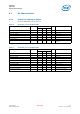
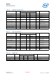
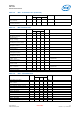
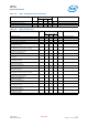
Table Of Contents
- 1.0 General Device Overview
- 2.0 Basic Operating Information
- 3.0 eUniStone Interfaces
- 4.0 General Device Capabilities
- 5.0 Bluetooth Capabilities
- 6.0 Electrical Characteristics
- 7.0 Package Information
- 8.0 Bluetooth Qualification and Regulatory Certification
- 8.1 Reference Design
- 8.2 FCC Class B Digital Devices Regulatory Notice
- 8.3 FCC Wireless Notice
- 8.4 FCC Interference Statement
- 8.5 FCC Identifier
- 8.6 European R&TTE Declaration of Conformity
- 8.7 Bluetooth Qualified Design ID
- 8.8 Industry Canada Certification
- 8.9 Label Design of the Host Product
- 8.10 Regulatory Test House
- 9.0 Assembly Guidelines
- References
- Terminology

eUniStone
PBA 31309
Electrical Characteristics
User’s Manual Intel Public 24
Hardware Description Revision 1.0, 1-Feb-2013
Table 8. VDDUART Supplied Pins
Parameter Symbol Values Unit Note / Test Condition
Min. Typ. Max.
Input low voltage -0.3 – 0.2*VDDUART V –
Input high voltage 0.7*VDDUART – VDDUART+0.3 V P0.5/UARTRXD
Input high voltage 0.7*VDDUART – 3.6 V Other pins
Output low voltage – – 0.25 V IOL = 5 mA
VDDUART = 2.5 V
Output low voltage – – 0.15 V IOL = 2 mA
VDDUART = 2.5 V
Output high voltage VDDUART
-0.25
–– VIOH=-5mA
VDDUART = 2.5 V
Output high voltage VDDUART
-0.15
–– VIOH=-2mA
VDDUART = 2.5 V
Continuous Load
1
1. The total continuous load for all VDDUART supplied pins shall not exceed 35 mA at the same time
––5 mA–
Pin Capacitance – – 10 pF –
Magnitude Pin Leakage – 0.01 1 µA Input and output drivers
disabled
Table 9. VDD1 Supplied Pins
Parameter Symbol Values Unit Note / Test Condition
Min. Typ. Max.
Input low voltage -0.3 – 0.2*VDD1 V –
Input high voltage 0.7*VDD1 – 3.6 V –
Output low voltage – – 0.25 V IOL = 5 mA
VDD1 = 2.5 V
Output low voltage – – 0.15 V IOL = 2 mA
VDD1 = 2.5 V
Output high voltage VDD1
-0.25
–– VIOH=-5mA
VDD1 = 2.5 V
Output high voltage VDD1
-0.15
–– VIOH=-2mA
VDD1 = 2.5 V
Continuous Load
1
1. The total continuous load for all VDD1 supplied pins shall not exceed 35 mA at the same time
––5 mA–
Pin Capacitance – – 10 pF –
Magnitude Pin Leakage – 0.01 1 µA Input and output drivers
disabled
Table 10. ONOFF PIN
Parameter Symbol Values Unit Note / Test Condition
Min. Typ. Max.
Input low voltage – – 0.7 V –
Input high voltage 1.7 – VSUPPLY V –
Input current -1 0.01 1 µA ONOFF = 0 V