WIRELESS DOCUMENTATION IA ISM-UGRP ISM Band Repeater Demo User Guide Version 2.0r - PRELIMINARY IA ISM-UGRP Rev 2.0r 1205 © 2005, Integration Associates, Inc.
Integration Associates, Inc. 110 Pioneer Way, Unit L Mountain View, California 94041 Tel: 650.969.4100 Fax: 650.969.4582 www.integration.com marketing@integration.com techsupport@integration.com ISM Band Repeater Demo User Guide Version 2.0r - Preliminary Revision Date: December 15, 2005 The information is provided “as is” without any express or implied warranty of any kind, including warranties of merchantability, non-infringement of intellectual property, or fitness for any particular purpose.
ABOUT THIS GUIDE The ISM Band Repeater Demo is designed to show the use of Integration's IA4220/IA4221/IA4320/IA4420 chipsets in a multi-transmitter/receiver environment. For further information on the devices found in this user guide, please visit our Web site: http://www.integration.
TABLE OF CONTENTS Demo Kit Contents ................................................................................................................................................. 1 Overview ...................................................................................................................................................................2 Repeater Demo Description ................................................................................................................................
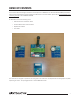
DEMO KIT CONTENTS This document describes designs available on the development kit CDROM for the 434 and 915 MHz ISM Repeater Demo. Also covered are the diagrams for both LCD and non-LCD variants. For further details, please refer to www.integration.com/ evaluation_kits.php or the IA ISM-DKxx CDROM.
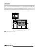
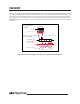
OVERVIEW The demo’s main objective is to show the IA4420’s capability to monitor multiple frequencies, receive data from an FSK transmitter, and then re-transmit this data on an another arbitrary frequency to another receiver or transceiver. This demonstration is designed to show the IA4420 acting as a repeater node.
OVERVIEW The demo uses the developer-friendly features of the IA4420 device. In receive mode the microcontroller reads the received bytes from the IA4420’s FIFO, and transmits them through the TX latch. This approach dramatically reduces the load on the micro, because the microcontroller doesn’t have to monitor every bit, only the bytes. This means the timing constraints in an application can be reduced at least by a factor of eight for both the transmitting and the receiving sides.
DESCRIPTION The frequency configuration of this demo is as follows: • One of the Push Button Demo receivers is set to a different frequency than that of the Push Button transmitter. The other receiver is paired with the frequency of the transmitter. • The Repeater demo receiving frequency is set to the frequency of the Push Button demo transmitter. The Repeater demo transmitting frequency is set to the non-paired Push Button demo receiver’s frequency .
Demo Unit TABLE OF CONTENTS Radio Hardware Stage 1 – IA4220 Transmitter Stage 2 – IA4420 Transceiver Stage 3 – IA4320 Receiver 5
This page is intentionally left blank 6
Radio Hardware IA4220/21 TRANSMITTER SECTION Contents - Schematic - 434 MHz Layouts - 915 MHz Layouts 7
SCHEMATIC: PUSH BUTTON DEMO TX BOARD 3 WP\ SO 2 GND 10u C1 VCC 8 B1 C3 GND R5 3k3 R4 SO 470 R1 R3 VCC GND 3k3 100p 100n - R2 10 k C2 6k8 + D1 HOLD\ SCK SI CS\ VCC 1 2 3 7 6 5 1 SCK SI CS SW1 EEPROM Array 4 VCC IC2 IC1 1 2 3 4 5 6 7 SCK VDD SEL IRQ WS1 RFP WS2 RFN WS3 MOD WS4 VSS CLK/SDO XTL 16 15 14 13 12 11 10 9 GND 1 2 FSK 3 4 SMDRET S4 1 2 3 4 SMDRET S3 1 2 3 4 SMDRET S2 1 2 3 4 SMDRET S1 8 SDI XTL 10 MHz LED 1 GND Fig 4.
PCB LAYOUT: 434 MHZ PUSH BUTTON TX BOARD Fig 5. 434 MHz Push Button Transmitter Board PCB Layout Fig 6.
PCB LAYOUT: 915 MHZ PUSH BUTTON TX BOARD Fig 7. 915 MHz Push Button Transmitter Board PCB Layout Fig 8.
Radio Hardware IA4420 TRANSCEIVER SECTION Contents - 50 Ohm Transceiver LCD Board - 50 Ohm Transceiver Non-LCD Board 11
1 2 3 POWER SERIAL GND GND 2,2uF C3 GND 3 TX 2 RX 1 FFS FFIT INT/VDI ARSSI SCK MISO MOSI IRQ R8 22 21 20 19 18 17 16 15 IC3 OUT 5 IA2112-3.3V GND VDD /RST/C2CK 3 ON POK 4 2 GND 1 IN P2.0 P2.1 P2.2 P2.3 P2.4 P2.5 P2.6 P2.7 P3.0/C2D C8051F311 P1.0 P1.1 P1.2 P1.3 P1.4 P1.5 P1.6 P1.7 P0.0 P0.1 P0.2 P0.3 P0.4 P0.5 P0.6 P0.
PCB LAYOUT: 50 OHM REPEATER DEMO (LCD VERSION) Fig 10. 50 Ohm Repeater Demo PCB Layout Fig 11.
VCC R1 GND R2 1 2 6V BATTERY J1 GND GND 3 TX 2 RX 1 FFS FFIT INT/VDI ARSSI SCK MISO MOSI IRQ 22 21 20 19 18 17 16 15 2,2uF C3 TX RX P3.0/C2D P1.0 P1.1 P1.2 P1.3 P1.4 P1.5 P1.6 P1.7 OUT 5 IA2112-3.3V 3 ON POK 4 2 GND 1 IN IC3 C8051F311 GND VDD /RST/C2CK P2.0 P2.1 P2.2 P2.3 P2.4 P2.5 P2.6 P2.
PCB LAYOUT: 50 OHM REPEATER DEMO (NON-LCD) Fig 13.
This page is intentionally left blank 16
Radio Hardware IA4320 RECEIVER SECTION Contents - Schematic - 434 MHz Layouts - 915 MHz Layouts 17
SCHEMATIC: 434 MHZ PUSH BUTTON RX BOARD 0R 0R R6 R5 GND GND C3 C2 C1 2 10u 10n 10p 3 4 5 7 LED4 RED LED3 RED LED2 RED LED1 RED 6 8 FCS0 FCS3 FBS0 FCS2 FBS1 VDD OUT0 IN1 OUT1 IN2 OUT2 VSS OUT3 FCS1 LPDM XTL VDD VDD 13 12 11 10 - GND G1 SW1 1 2 3 GND GND GND GND 14 GND B2430UNI + 15 9 IA4320 470 470 R1 470 R2 470 R3 R4 GND 16 XTAL 1 10MHz VDD IC GND Fig 15.
PCB LAYOUT: 434 MHZ PUSH BUTTON RX BOARD Lit.3V 0x20,3 10,2x17,8 7,5x20,3 10,2x20,3 Fig 16. 434 MHz Push Button Receiver Board PCB Layout Fig 17.
SCHEMATIC: 915 MHZ PUSH BUTTON RX BOARD 2 2 10uF 10n 10p 3 1 3 FCS0 4 GND 2 FCS1 1 FCS3 2 LPDM 3 1 LPDM RED LED4 RED LED3 1 3 R4 470 2 FCS3 R3 470 1 FCS2 RED LED2 3 6 RED LED1 2 FCS2 R2 470 FCS1 R1 470 3 5 GND GND GND GND 7 LPDM 8 IC FCS0 FBS0 FCS2 FBS1 VDD OUT0 OUT1 OUT2 OUT3 LPDM POWER 2 1 FCS3 IN1 IN2 VSS FCS1 XTL VDD VDD=2.2V - 5.
PCB LAYOUT: 915 MHZ PUSH BUTTON RX BOARD Fig 18. 915 MHz Push Button Receiver Board PCB Layout Fig 19.
Integration Associates, Inc. 110 Pioneer Way, Unit L Mountain View, California 94041 Tel: 650.969.4100 Fax: 650.969.4582 www.integration.com info@integration.com techsupport@integration.com P694 This document may contain preliminary information and is subject to change by Integration Associates, Inc. without notice. Integration Associates assumes no responsibility or liability for any use of the information contained herein.