
Data Sheet


Preliminary Data Sheet
April 23, 2020
Page 15/25
Document Ref: isp_ble_DS1907_R4.docx
Insight SiP
– Green Side – 400 avenue Roumanille – BP 309 – 06906 Sophia-Antipolis Cedex – France –
www.insightsip.com
BLE MODULE
ISP1907
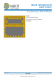
4.2. SMT Assembly Guidelines
For PCB Land Patterns and Solder Mask layout, Insight SiP recommends to use the same dimensions as
module pads, ie 0.4 x 0.4 mm for standard pads and 0.8 x 0.8 mm for corner pads.
Please contact Insight SiP for more detailed information.
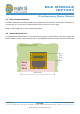
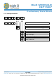
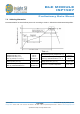
4.3. Antenna Keep-Out Zone
For optimal antenna performance, it is recommended to respect a metal exclusion zone to the edge of the
board:no metal, no traces and no components on any application PCB layer except mechanical LGA pads.
Application PCB
Keep
Out
Zone
18.0 mm min
4.0
mm
1
Specification subject to change without notice.