
Datasheet


I
C
,
nom
50 A
I
C
75 A
min. typ. max.
- 1,7 2,15 V
- 2,0 - V
I²t value
I²t
V
GE(th)
C
ies
nA
gate emitter leakage current
Gate Emitter Reststrom
V
CE
= 0V, V
GE
= 20V, T
vj
= 25°C I
GES
- 400
6,5
-
-
- 5
0,13 -
V
nF3,50
-
0,47
-
µC
A
DC forward current
+
20
700 A²s
t
p
= 1ms I
FRM
100 A
Grenzlastintegral
100
Dauergleichstrom
I
F
50
T
c
= 25°C; Transistor
repetitive peak collector current
t
p
= 1ms, T
c
= 80°C
Periodischer Kollektor Spitzenstrom
W
V
gate emitter peak voltage
T
c
= 25°CDC collector current
Höchstzulässige Werte / maximum rated values
Kollektor Emitter Sperrspannung
T
c
= 80°CKollektor Dauergleichstrom
collector emitter voltage
T
vj
= 25°C
1200 V
Elektrische Eigenschaften / electrical properties
I
C
= 50A, V
GE
= 15V, T
vj
= 125°C
Gate Schwellenspannung
I
C
= 2,0mA, V
CE
= V
GE
, T
vj
= 25°C
gate threshold voltage
Periodischer Spitzenstrom
Gesamt Verlustleistung
total power dissipation
Gate Emitter Spitzenspannung
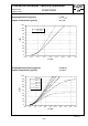
V
CEsat
Charakteristische Werte / characteristic values
approved: SM TM; Robert Severin
V
R
= 0V, t
p
= 10ms, T
vj
= 125°C
Technische Information / technical information
FS50R12KE3
IGBT-Module
IGBT-Modules
V
CES
A
Isolations Prüfspannung
insulation test voltage
RMS, f= 50Hz, t= 1min.
V
ISOL
I
CRM
P
tot
270
repetitive peak forward current
kV2,5
5,0 5,8
Transistor Wechselrichter / transistor inverter
date of publication: 2002-09-03
Kollektor Emitter Sättigungsspannung
I
C
= 50A, V
GE
= 15V, T
vj
= 25°C
collector emitter saturation voltage
V
GES
revision: 3.0
Eingangskapazität
input capacitance
f= 1MHz, T
vj
= 25°C, V
CE
= 25V, V
GE
= 0V
prepared by: MOD-D2; M. Münzer
collector emitter cut off current
I
CES
Rückwirkungskapazität
reverse transfer capacitance
f= 1MHz, T
vj
= 25°C, V
CE
= 25V, V
GE
= 0V
Kollektor Emitter Reststrom
C
res
mA-
V
CE
= 1200V, V
GE
= 0V, T
vj
= 25°C
Gateladung
V
GE
= -15V...+15V Q
G
-
gate charge
nF -
1 (8)
DB_FS50R12KE3_ 3.0.xls
2002-09-03