
Datasheet
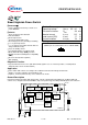


PROFET
®
BTS 6163 D
Data Sheet 4 of 18 Rev. 1.0, 2007-07-23
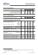
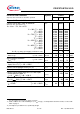
Values Parameter and Conditions
at T
j
= 25, V
bb
= 24 V unless otherwise specified
Symbol
min. typ. max.
Unit
Operating Parameters
Operating voltage (VIN=0) T
j
=-40...150 °C: V
bb(on)
5.5 -- 62 V
Undervoltage shutdown
7) 8)
V
bIN(u)
-- 2.5 3.5 V
Undervoltage restart of charge pump
V
bb(ucp)
-- 4 5.5 V
Overvoltage protection
9)
I
bb
=15 mA
V
Z,IN
68
73
-- V
Standby current T
j
=-40...+120°C:
I
IN
=0 T
j
=150°C:
I
bb(off)
--
--
3
6
6
14
µA
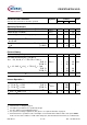
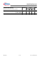
Reverse Battery
Reverse battery voltage
10)
-V
bb
-- -- 16 V
On-state resistance (pin 1,5 to pin 3)
V
bb
= - 8V, V
IN
= 0, I
L
= -7.5 A, R
IS
= 1 kΩ,
8)
T
j
=25 °C:
T
j
=150 °C:
V
bb
= -12..-24V, V
IN
= 0, I
L
= -7.5 A, R
IS
= 1 kΩ,
T
j
=25 °C:
T
j
=150 °C:
R
ON(rev)
--
--
--
--
19
35
18
33
25
44
23
40
mΩ
Integrated resistor in V
bb
line R
bb
-- 100 150 Ω
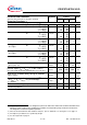
Inverse Operation
11)
Output voltage drop (pin 1,5 to pin 3)
8)
I
L
= -7.5 A, R
IS
= 1 kΩ, T
j
=25 °C:
I
L
= -7.5 A, R
IS
= 1 kΩ, T
j
=150 °C:
-V
ON(inv)
--
--
700
300
--
--
mV
Turn-on delay after inverse operation; I
L
> 0A
8)
V
IN
(inv) = V
IN
(fwd) = 0 V
t
d(inv)
--
1 -- ms
7)
VbIN=Vbb-VIN see diagram page 14.
8)
Not subject to production test, specified by design.
9)
See also V
ON(CL)
in circuit diagram page 9.
10)
For operation at voltages higher then |16V| please see required schematic on page 10.
11)
Permanent Inverse operation results eventually in a current flow via the intrinsic diode of the power DMOS.
In this case the device switches on with a time delay t
d(inv)
)
after the transition from inverse to forward mode.