
Datasheet

Data Sheet 8 Rev. 2.1, 2010-11-22
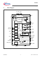
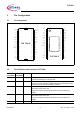
TLE7368
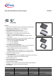
Pin Configuration
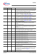
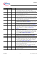
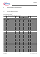
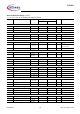
22 23 SEL_LDO2 Selection input LDO2;
Connect to GND to select 2.6 V output voltage for LDO2;
Connect straight to Q_LDO2 to select 3.3 V output voltage for LDO2.
23 24 WDI Window Watchdog input;
Apply a watchdog trigger signal to this pin
24 25 WDO Window Watchdog output;
Open drain output, active low,
connect external 10 kΩ pull-up resistor to microcontroller I/O voltage
25, 26 26, 27 SW Buck power stage’s output;
Connect both pins directly, on short lines, to the Buck converter circuit,
i.e. the catch diode and the Buck inductance
27 28 BST Bootstrap driver supply input;
Connect the buck power stage’s driver supply capacitor to the SW pins;
For capacitor selection please refer to Chapter 6.
28 29 FB/L_IN Buck converter feedback input plus input for LDO1 and trackers;
Connect the output of the buck converter circuit with short lines to these
pins; For Buck output capacitor selection please refer to Chapter 6.
29 30 Q_LDO1 Voltage regulator 1 output;
5 V output; Block to GND with capacitor for stable regulator operation;
Selection of capacitor
C
Q_LDO1
according to Chapter 4.4 and
Chapter 6.
30 31 FB_EXT External regulator feedback input;
Feedback input of control loop for the external power stage regulator.
Connect to the emitter of the regulating transistor; Block to GND with
capacitor for stable regulator operation; Selection of capacitor
C
Q_FB_EXT
according to Chapter 4.4 and Chapter 6.
31 32 DRV_EXT Bipolar power stage driver output;
Connect the base of an external NPN transistor directly to this pin;
Regarding choice of the external power stage refer to Chapter 6.
32, 33 – N.C. Internally not connected; Connect to GND_A.
34 33 Q_STBY Stand-by regulator output;
Output voltage depending on the state of SEL_STBY; Block to GND
with capacitor for stable regulator operation; Selection of capacitor
C
Q_STBY
according to Chapter 4.4 and Chapter 6.
35 34 IN_STBY Input to stand-by regulator;
Always connect the reverse polarity protected battery line to this pin;
Input to all IC internal biasing circuits;
Block to GND directly at the IC with ceramic capacitor; For proper
choice of input capacitors please refer to Chapter 6.
36 35 MON_STBY Monitoring output for stand-by regulator; power fail active low
output with special timing, open drain, connect external pull-up resistor.
– 36 GND_A Analog ground connection;
Connect to exposed pad.
Pin
(TLE7368G)
Pin
(TLE7368E)
Symbol Function