
Datasheet

TLE7368
Detailed Internal Circuits Description
Data Sheet 25 Rev. 2.1, 2010-11-22
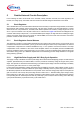
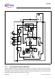
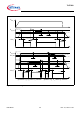
Figure 3 Buck Converter Block Diagram
5.1.3 Electromagnetic Emission Reduction
The Buck DMOS power stage is implemented as multiple cells. This allows to control the slope of the power
stage’s current at turn on/off by sequentially turning on/off the cells, achieving a smooth turn on/off and therefore
avoiding high frequency components in the electromagnetic emissions to the battery line. The current slope control
is adjusted internally, the typical current slew rate is 50 ns/A.
+
-
+
-
QS
R
+
-
+
-
+
-
&
OTSD
Charge pump
Bootstrap
charger
BST
SW
FB/L_IN
CCPC2-C2+C1-C1+
IN
Error
amplifier
Current
comparator
Over temp.
shutdown
Oscillator
Slope
compensation
Current sense
amplifier
Over voltage
shutdown
Level
shifter
Level
shifter
Slope
control
Under voltage
shutdown
High side
driver
DMOS power
stages