
Datasheet

TLE7368
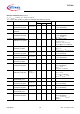
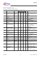
General Product Characteristics
Data Sheet 13 Rev. 2.1, 2010-11-22
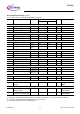
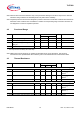
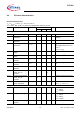
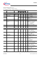
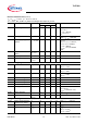
4.4 Electrical Characteristics
Electrical Characteristics
V
IN
= V
IN_STBY
= 13.5 V, T
j
= -40 °C to +150 °C,
V
CCP
= 9.0 V; SEL_STBY = Q_STBY; all voltages with respect to ground.
Pos. Parameter Symbol Limit Values Unit Conditions
Min. Typ. Max.
Buck Regulator
4.4.1 Switching frequency
f
280 370 425 kHz –
4.4.2 Current transition
rise/fall time
t
r, I
–50–ns
1)
; slope magnitude 1 A; fixed
internally
4.4.3 Power stage on
resistance
R
ON, Buck
––280mΩ –
4.4.4 Power stage peak
current limit
I
peak, SW
2.5 – 4.6 A V
IN
= 5.0 V;
V
SW
ramped down from 5.0 V
to 3.7 V;
V
FB/L_IN
= 5.0 V
4.4.5 Buck converter output
voltage
V
FB/L_IN
5.4 – 6.0 V I
Buck
= 2.0 A
2)
4.4.6 Buck converter output
voltage
V
FB/L_IN
5.4 – 6.4 V I
Buck
= 100 mA
2)
4.4.7 Buck converter, turn on
threshold
V
IN, on
––4.5VV
IN
increasing
4.4.8 Buck converter, turn off
threshold
V
IN, off
3.5 – – V V
IN
decreasing
4.4.9 Buck converter On/off
hysteresis
V
IN, hyst
450 500 550 mV V
IN, hyst
= V
IN, on
- V
IN, off
4.4.10 Bootstrap undervoltage
lockout, turn on
threshold
V
BST_UV, on
––V
SW
+
5.0
V Bootstrap voltage increasing
4.4.11 Bootstrap undervoltage
lockout, turn off
threshold
V
BST_UV, off
V
SW
+
3.2
– – V Bootstrap voltage decreasing
4.4.12 Bootstrap undervoltage
lockout, hysteresis
V
BST_UV, hyst
0.2 – 1 V V
BST_UV, hyst
=
V
BST_UV, on
- V
BST_UV, off
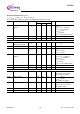
Charge Pump
4.4.13 Charge pump voltage
V
CCP
9–15VC
C1
= 100 nF;
C
C2
= 100 nF;
C
CCP
= 220 nF
4.4.14 Charge pump voltage
V
CCP
9–13.5VV
IN
= 4.5 V;
C
C1
= 100 nF;
C
C2
= 100 nF;
C
CCP
= 220 nF
4.4.15 Charge pump switching
frequency
f
CCP
1.0 – 2.5 MHz –