
Datasheet

Data Sheet 12 Rev. 2.1, 2010-11-22
TLE7368
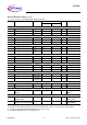
General Product Characteristics
Note: Stresses above the ones listed here may cause permanent damage to the device. Exposure to absolute
maximum rating conditions for extended periods may affect device reliability.
Note: Integrated protection functions are designed to prevent IC destruction under fault conditions described in the
data sheet. Fault conditions are considered as “outside” normal operating range. Protection functions are
not designed for continuous repetitive operation.
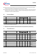
4.2 Functional Range
Note: Within the functional range the IC operates as described in the circuit description. The electrical
characteristics are specified within the conditions given in the related electrical characteristics table.
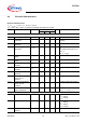
4.3 Thermal Resistance
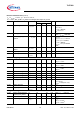
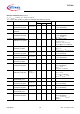
Pos. Parameter Symbol Limit Values Unit Conditions
Min. Max.
4.2.1 Stand-by input voltage
V
IN_STBY
3.0 45 V
1)
1) At minimum battery voltage regulators with higher nominal output voltage will not be able to provide the full output voltage.
Their outputs follow the battery with certain drop.
4.2.2 Buck input voltage V
IN
4.5 45 V
1)
4.2.3 Peak to peak ripple voltage at
FB/L_IN
V
FB/L_IN
0 150 mVpp –
4.2.4 Junction temperature
T
j
-40 150 °C–
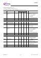
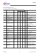
Pos. Parameter Symbol Limit Values Unit Conditions
Min. Typ. Max.
Power-P-DSO-36
4.3.1 Junction to ambient
R
thJA
– 49 – K/W Footprint only
1)
1) Worst case regarding peak temperature; zero airflow; mounted on FR4; 80 × 80 × 1.5 mm
3
; 35µ Cu; 5µ Sn
4.3.2 Junction to ambient R
thJA
– 39 – K/W Heat sink area
300mm
2
1)
4.3.3 Junction to ambient R
thJA
– 32 – K/W Heat sink area
600mm
2
1)
4.3.4 Junction to case R
thJC
–4.4–K/W–
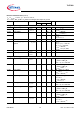
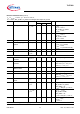
PG-DSO-36
4.3.5 Junction to ambient
R
thJA
– 54 – K/W Footprint only
1)
4.3.6 Junction to ambient R
thJA
– 42 – K/W Heat sink area
300mm
2
1)
4.3.7 Junction to ambient R
thJA
– 35 – K/W Heat sink area
600mm
2
1)
4.3.8 Junction to case R
thJC
–5.6–K/W–