
Datasheet

TLE7368
General Product Characteristics
Data Sheet 11 Rev. 2.1, 2010-11-22
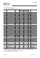
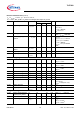
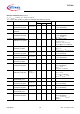
Feedback and Post-Regulators Input FB/L_IN
4.1.52 Voltage
V
FB/L_IN
V
Q_LDO1
- 0.3 18 V –
4.1.53 Voltage
V
FB/L_IN
-0.3 18 V –
4.1.54 Current
I
FB/L_IN
– – A Limited internally
Linear Regulator 2 Input IN_LDO2
4.1.55 Voltage
V
IN_LDO2
V
Q_LDO2
- 0.3 18 V –
4.1.56 Voltage
V
IN_LDO2
-0.3 18 V –
4.1.57 Current
I
IN_LDO2
– – A Limited internally
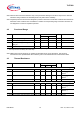
Bootstrap Supply BST
4.1.58 Voltage
V
BST
V
SW
- 0.3 V
SW
+ 5.5 V –
4.1.59 Voltage
V
BST
-0.3 51 V –
4.1.60 Current
I
BST
– – A Limited internally
Buck Power Stage SW
4.1.61 Voltage
V
SW
-2 V
IN
+ 0.3 V –
4.1.62 Voltage
V
SW
-2 45 V –
4.1.63 Current
I
SW
– – A Limited internally
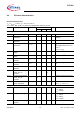
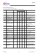
Stand-by Regulator Output Q_STBY
4.1.64 Voltage
V
Q_STBY
-0.3 5.5 V –
4.1.65 Voltage
V
Q_STBY
-0.3 6.2 V t < 10 s
2)
4.1.66 Current I
Q_STBY
– – A Limited internally
Monitoring Output MON_STBY
4.1.67 Voltage
V
MON_STBY
-0.3 5.5 V –
4.1.68 Voltage
V
MON_STBY
-0.3 6.2 V t < 10 s
2)
4.1.69 Current I
MON_STBY
– – A Limited internally
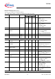
Temperatures
4.1.70 Junction Temperature
T
j
-40 150 °C–
4.1.71 Storage Temperature
T
stg
-50 150 °C–
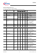
ESD-Protection (Human Body Model)
4.1.72 Electrostatic discharge
voltage
V
ESD
-2 2 kV Human Body Model
(HBM)
3)
ESD-Protection (Charged Device Model)
4.1.73 Electrostatic discharge
voltage to GND
V
ESD
-500 500 V Charged Device
Model (CDM)
4)
4.1.74 Electrostatic discharge
voltage, corner pins to GND
V
ESD
-750 750 V Charged Device
Model (CDM)
4)
1) Not subject to production test, specified by design.
2) Exposure to those absolute maximum ratings for extended periods of time (
t > 10 s) may affect device reliability.
3) According to JEDEC standard EIA/JESD22-A114-B (1.5 kΩ, 100 pF)
4) According to EIA/JESD22-C101 or ESDA STM5.3.1
Absolute Maximum Ratings (cont’d)
1)
T
j
= -40 °C to +150 °C; all voltages with respect to ground.
Pos. Parameter Symbol Limit Values Unit Conditions
Min. Max.