
Datasheet

TLE 7241E
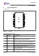
Pin Configuration
Data Sheet 7 Rev. 1.1, 2009-01-19
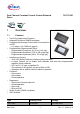
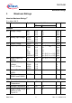
2 Pin Configuration
Pin Assignment
PINOUT. VSD
TLE 7241E
PGND1
OUT1
POS1
NEG1
PGND2
OUT2
POS2
NEG2
BAT
GND
SCK
VDD
CSB
SI
REF
TEST
DEFAULT
SO
VSO
N.C.
1
2
3
4
5
6
7
8
9
10
20
19
18
17
16
15
14
13
12
11
EPGND
Figure 3Pin-Out
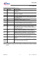
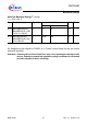
Pin Definitions and Functions
Pin Pin Name Pin Description
1 PGND1 Power Ground Channel 1; internally connected to
PGND2
2 OUT1 Output Channel 1; Drain of Output DMOS; connect to
negative terminal of external sense resistor
3 NEG1 Negative Sense Pin Channel 1; connect to negative
terminal of external sense resistor with dedicated trace
4 POS1 Positive Sense Pin Channel 1; connect to positive
terminal of external sense resistor with dedicated trace
5 NC Not Connected; not bonded internally
6 V
DD
Logic Supply Voltage; connect a ceramic capacitor to
GND near the device
7 DEFAULT Control Input; Active high digital input. 3.3V and 5.0V
logic compatible. In case of not used, connect to ground