
Datasheet

Data Sheet 66 Rev. 1.1, 2009-01-19
TLE 7241E
Application
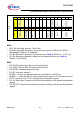
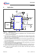
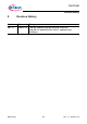
6 Application
TLE7241
BAT
GND
NEG1
OUT1
POS1
DEFAULT
VSO
SI
SO
SCK
VDD
REF
NEG2
OUT2
POS2
CSB
Rsns1
VPWR/
RECIRC
Cbat
Cref
Cng1
(3)
Cps1
(3)
Csol1
Cvdd
SOL1
VPWR
+5V
2.5V ref
Rsns2
VPWR/
RECIRC
Cng2
(3)
Cps2
(3)
Cout2 (3)
Csol2
SOL2
Cout1(3)
Cso
+5V or 3.3V
μController
Tri-Core
TC17XX
Rso
(5)
TEST
PGND1
PGND2
Rbat (2)
(4)
Rdft (1).
Figure 30 Application Circuit
Note: This is a very simplified example of an application circuit. The function must be
verified in the real application
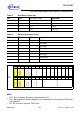
1. Recommended for applications with microcontroller I/O voltage levels less than
5.0 V. The resistor will limit the microcontroller input current when the adjacent pins
DEFAULT and
V
DD
are shorted together.
2. Required for applications that do not provide a reverse battery protected BAT supply.
R
BAT
may also be required to limit the BAT pin current during BAT voltage transient
events (e. g. ISO pulses).
3. May be required for module level compliance with EMC specifications, but they are
not required for TLE7241 functionality or stability.
4. Connect to the REF pin directly to GND to enable the internal 2.5 V voltage reference.
5. Optional. Defines SO signal voltage when the SO pin has failed as an open circuit.
Note: In case of an unused channel, the OUTx, NEGx, and POSx pins should be
connected together.