
Datasheet


TLE 7241E
Functional Description and Electrical Characteristics
Data Sheet 51 Rev. 1.1, 2009-01-19
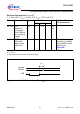
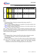
Figure 24 Fault Bit Refresh Delay Time (t
dly
)
5.6.1.23 SCK
Number of
SCK pulses
while CSB low
(n is a positive
integer)
n
SCK
16 n × 16 – Pul-
ses
–
5.6.1.24 CSB
3)
MISO shift
register load
delay time
t
dly
– 1.7 – μs CSB = 2.0 V
(increasing) to MISO
data loaded into shift
register (see
Figure 24)
Latched
Fault Bit
CSB
Tdly
1) Positive current flow is into the device.
2)
T
J
= 25 °C.
3) Not subject to production test, specified by design.
Electrical Characteristics (cont’d)
1)
T
j
= -40 to 150 °C; V
BAT
= 9 V to 18 V; V
DD
= 4.75 V to 5.25 V
Pos. Parameter Symbol Limit Values Unit Test Conditions
and Instructions
Min. Typ.
2)
Max.