
Datasheet

TLE 7241E
Functional Description and Electrical Characteristics
Data Sheet 49 Rev. 1.1, 2009-01-19
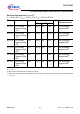
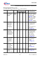
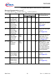
5.6.1.10 SO, CSB SO
Pin Enable/
Disable
Tsoen,
Tsodis
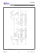
– – 80 ns CSB = 2.0 V to SO =
0.8 V/2.0 V, 10K ext.
SO pull-up (see
Figure 23) - enable
CSB = 0.8 V to SO
hi-Z, 10K ext. SO
pull-up (see
Figure 23) - disable
5.6.1.11 SO, SCK
3)
Output Data
Setup Time,
SO to SCK
Rising Edge
T
su1
80 – – ns Required setup time
by microprocessor
equivalent to T
wl
-
T
valid
SO = 0.8 V/2.0 V to
SCK = 0.8 V
(see Figure 23)
5.6.1.12 SO, SCK
3)
Output Data
Hold Time, SO
Hold After SCK
Rising Edge
T
h1
150 – – ns Required hold time
by microprocessor
equivalent to T
wh
+
T
valid
- T
rso
/T
fso
SCK = 2.0 V to
SO
= 0.8 V/2.0 V
(see Figure 23)
5.6.1.13 SI, SCK Input
Data Setup
Time, SI to
SCK Rising
Edge
T
su2
20 – – ns SI = 0.8 V/2.0 V to
SCK = 2.0 V at
3.2 MHz
(see Figure 23)
5.6.1.14 SI, SCK Input
Data Hold
Time, SI Hold
after SCK
Rising Edge
T
h2
30 – – ns SCK = 2.0 V to
SI = 0.8 V/2.0 V at
3.2 MHz
(see Figure 23)
5.6.1.15 SO Serial
Output
Rise/Fall Time
T
rso
/T
fso
– – 50 ns C
ld
= 200 pF
(see Figure 23)
Electrical Characteristics (cont’d)
1)
T
j
= -40 to 150 °C; V
BAT
= 9 V to 18 V; V
DD
= 4.75 V to 5.25 V
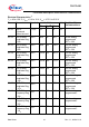
Pos. Parameter Symbol Limit Values Unit Test Conditions
and Instructions
Min. Typ.
2)
Max.