
Datasheet

Data Sheet 48 Rev. 1.1, 2009-01-19
TLE 7241E
Functional Description and Electrical Characteristics
Electrical Characteristics
1)
T
j
= -40 to 150 °C; V
BAT
= 9 V to 18 V; V
DD
= 4.75 V to 5.25 V
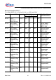
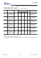
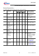
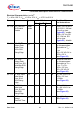
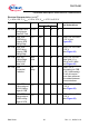
Pos. Parameter Symbol Limit Values Unit Test Conditions
and Instructions
Min. Typ.
2)
Max.
5.6.1.1 CSB Input Bias
Current
I
CSB
-25 -10 -5 μA V
CSB
= 0 V
Pull-up source is
from pin V
SO
5.6.1.2 SI Input Pull-
down Current
I
SI
5 10 25 μA V
SI
= V
VSO
5.6.1.3 SCK Input Pull-
down Current
I
SCK
5 10 25 μA V
SCK
= V
VSO
5.6.1.4 SO Tri-state
Leakage
Current
I
SOT
-10 0 10 μA CSB = 0.7 V
DD
0 V < V
SO
< V
VSO
5.6.1.5 SI, SCK, CSB,
DEFAULT
Input
Capacitance
C
IN
– – 20 pF 0 V < V
SO
< 5.25 V
3)
5.6.1.6 SO Tri-state
Output
Capacitance
C
SOT
– – 20 pF 0 V < V
SO
< 5.25 V
3)
5.6.1.7 SCK Serial
Clock
Frequency
f
SCK
– – 3.2 MHz SPI clock
SPI communications
tested at C
L
= 200 pF
on the SO pin,
T
su1
= 40 ns
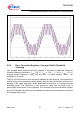
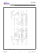
5.6.1.8 SCK Clock
Pulse High
Time
T
wh
85 – – ns f
SCK
= 3.2 MHz,
SCK = 2 V to 2 V
(see Figure 23)
5.6.1.9 SCK Clock
Pulse Low
Time
T
wl
85 – – ns f
SCK
= 3.2 MHz,
SCK = 0.8 V to 0.8 V
(see Figure 23)