
Datasheet

TLE 7241E
Functional Description and Electrical Characteristics
Data Sheet 31 Rev. 1.1, 2009-01-19
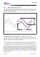
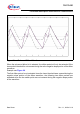
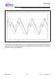
Note that the switching frequency and duty cycle of the output transistor are not directly
controlled by the TLE 7241E device and are dependent on the characteristics of the
solenoid (inductance, resistance, etc.) and the solenoid supply voltage.
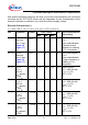
Electrical Characteristics
1)
T
j
= -40 to 150 °C; V
BAT
= 9 V to 18 V; V
DD
= 4.75 V to 5.25 V
Pos. Parameter Symbol Limit Values Unit Test Conditions and
Instructions
Min. Typ.
2)
Max.
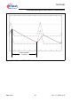
5.5.1.1 OUTx
3)
Blanking
time 1 (see
Figure 16,
Figure 17)
T
blank1
– 5 – μs Slew Rate Register =
0 or 1.
From enable/disable
of lowside output
transistor to enabling
of
V
pos
comparator.
5.5.1.2 OUTx
3)
Blanking
time 2 (see
Figure 16,
Figure 17)
T
blank2
– 15 – μs Slew Rate Register =
2 or 3.
From enable/disable
of output transistor to
enabling of
V
pos
comparator.
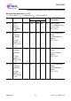
5.5.1.3 OUTx
4)5)
dV
OUT
=
200
mV
I
avg
register
= 0A6
H
dV
OUT 200
-5% 200 +5% mV Output current
I
OUT
= 200 mA with
R
sense
= 1.0 Ω
REF = 2.5V
5.5.1.4 OUTx
4)5)
dV
OUT
=
400
mV
I
avg
register
= 14D
H
dV
OUT 400
-2.5 % 400 2.5% mV Output current
I
OUT
= 400 mA with
R
sense
= 1.0 Ω
REF = 2.5V
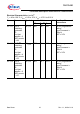
5.5.1.5 OUTx
4)5)
dV
OUT
=
600
mV
I
avg
register
= 1F3
H
dV
OUT 600
-2% 600 2% mV Output current
I
OUT
= 600 mA with
R
sense
= 1.0 Ω
REF = 2.5V
5.5.1.6 OUTx
4)5)
d
V
OUT
=
800 mV
I
avg
register
= 29A
H
dV
OUT 800
-2% 800 2% mV Output current
I
OUT
= 800 mA with
R
sense
= 1.0 Ω
REF = 2.5V