
Datasheet

Data Sheet 14 Rev. 1.1, 2009-01-19
TLE 7241E
Functional Description and Electrical Characteristics
5.2 Input/Output
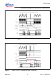
The DEFAULT pin is an active high input. A weak pull-up current (typical 15 μA) on this
pin ensures a defined level when this pin is not connected (e.g. open pin). An active high
signal on the DEFAULT pin sets the commanded current for both channels to 0 mA, and
resets all programmable registers to their default values. Any SPI commands that are
received while the DEFAULT pin is high will be ignored, and the SO pin will remain in a
high impedance state.
The fault register bits are not cleared when the Default pin is asserted.
Upon coming out of default mode, the commanded current will remain at 0 mA, device
off, and the programmable registers will remain at their default values.
The DEFAULT pin must be asserted high whenever the voltage on the pin V
DD
is less
than the minimum
V
DD
operating voltage (4.75 V), otherwise the electrical characteristic
specifications (see table below) may not be met. The diagnostic functions are not
operational when the
V
DD
voltage is less than 4.75V.
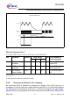
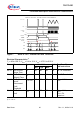
The TEST pin is an active high pin. This pin must be connected directly to ground in the
application, as it is only used for IC test purposes. A passive pull-down resistor in the
device ensures a logic low value when the pin is not connected.
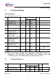
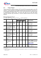
T
j
= -40 to 150 °C; V
BAT
= 9 V to 18 V; V
DD
= 4.75 V to 5.25 V
Pos. Parameter Symbol Limit Values Unit Test Conditions
and Instructions
Min.
2) Target @T
J
= 25 °C
Typ.
2)
DEFAULT
Input Bias Current
I
DEFAULT
-25 -10 -5 μA V
DEFAULT
= 0 V;
Pull-up source is pin V
SO
TEST
Pull-down Resistor
R
TEST
– 20 – kΩ –
SI, SCK, CSB,
DEFAULT Input
Threshold
V
IH
2.0 – – V SCK is specified by
design, not subject to
production test.
SI, SCK, CSB,
DEFAULT Input
Threshold
V
IL
– – 0.8 V SCK is specified by
design, not subject to
production test.
SO Output High
Voltage
V
OH
0.8
V
SO
– – V SO I
o
= -1 mA
SO Output Low
Voltage
V
OL
– – 0.4 V SO I
o
= 1 mA
Electrical Characteristics
1)
1) Positive current flow is into the device.
Max.
5.2.1
5.2.2
5.2.3
5.2.4
5.2.5
5.2.6