
Datasheet


Datasheet 9 Rev. 1.1, 2011-04-12
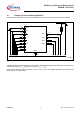
SPI Driver for Enhanced Relay Control
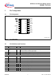
SPIDER - TLE7231G
General Product Characteristics
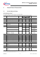
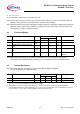
4 General Product Characteristics
4.1 Absolute Maximum Ratings
Absolute Maximum Ratings
1)
T
j
= -40 °C to +150 °C; V
DD
= 3.0 V to V
DDA
, V
DDA
= 4.5V to 5.5V.
All voltages with respect to ground, positive current flowing into pin (unless otherwise specified)
1) Not subject to production test, specified by design.
Pos. Parameter Symbol Limit Values Unit Conditions
Min. Max.
Power Supply
4.1.1 Digital supply voltage
V
DD
-0.3 5.5 V –
4.1.2 Analog supply voltage
V
DDA
-0.3 5.5 V –
Power Stages
4.1.3 Load current
I
D
-0.5 0.5 A –
4.1.4 Output voltage for short circuit protection
(single pulse)
V
D
–36V–
4.1.5 Voltage at power transistor
V
DS
– 41 V active clamped
4.1.6
Maximum energy dissipation one channel E
AS
mJ
2)
2) Pulse shape represents inductive switch off: I
D
(t) = I
D
(0) × (1 - t / t
pulse
); 0 < t < t
pulse
single pulse – 65 T
j(0)
= 85 °C
I
D(0)
= 0.35 A
single pulse – 30
T
j(0)
= 150 °C
I
D(0)
= 0.25 A
repetitive (1 · 10
4
cycles)
repetitive (1 · 10
6
cycles)
E
AR
–
–
18
13
T
j(0)
= 150 °C
I
D(0)
= 0.25 A
I
D(0)
= 0.17 A
Logic Pins
4.1.7 Voltage at input pin
V
IN
-0.3 5.5 V –
4.1.8 Voltage at reset pin
V
RST
-0.3 V
DD
+ 0.3 V
3)
4.1.9 Voltage at chip select pin V
CS
-0.3 V
DD
+ 0.3 V
3)
4.1.10 Voltage at serial clock pin V
SCLK
-0.3 V
DD
+ 0.3 V
3)
4.1.11 Voltage at serial input pin V
SI
-0.3 V
DD
+ 0.3 V
3)
4.1.12 Voltage at serial output pin V
SO
-0.3 V
DD
+ 0.3 V
3)
Temperatures
4.1.13 Junction Temperature during operation
T
j
-40 150 °C–
4.1.14 Dynamic temperature increase while
switching
∆T
j
–60°C–
4.1.15 Storage Temperature
T
stg
-55 150 °C–
ESD Susceptibility
4.1.16 ESD Resistivity
V
ESD
kV HBM
4)
Output -4 4
Input / SPI -2 2