
Datasheet


Datasheet 7 Rev. 1.1, 2011-04-12
SPI Driver for Enhanced Relay Control
SPIDER - TLE7231G
Pin Configuration
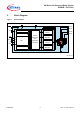
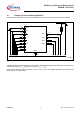
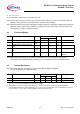
3 Pin Configuration
3.1 Pin Assignment
Figure 3 Pin Configuration
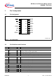
3.2 Pin Definitions and Functions
Pin Symbol I/O
1)
Function
Power Supply
10
V
DD
- Digital Supply Voltage; Connected to 5V Voltage with Reverse
protection Diode and Filter against EMC
12
V
DDA
- Analog Supply Voltage;
11,4 GND - Ground; common ground for digital, analog and power
Power Stages
14 OUT0 O Output Channel 0; Drain of power transistor channel 0
13 OUT1 O Output Channel 1; Drain of power transistor channel 1
9OUT2 OOutput Channel 2; Drain of power transistor channel 2
8OUT3 OOutput Channel 3; Drain of power transistor channel 3
Inputs
3IN IPDControl Input; Digital input 3.3 V or 5V. In case of not used keep open.
1RST
IPDReset input pin; Digital input 3.3 V or 5V. Low active
SPI
2CS
IPUSPI chip select; Digital input 3.3 V or 5V.Low active
7SCLK IPDserial clock; Digital input 3.3 V or 5V.
P-DSO-14 .em f
(top view)
OUT0
OUT1
VDDA
14
13
12
11
10
9
1
2
3
4
5
6
GND
78
OUT2
OUT3
VDD
GND
SI
SO
SCLK
IN
RST
CS