
Datasheet
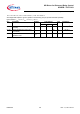

Datasheet 29 Rev. 1.1, 2011-04-12
SPI Driver for Enhanced Relay Control
SPIDER - TLE7231G
Application Information
10 Application Information
Note: The following information is given as a hint for the implementation of the device only and shall not be
regarded as a description or warranty of a certain functionality, condition or quality of the device.
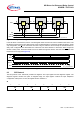
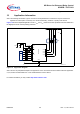
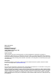
Figure 15 shows a simplified application circuit.
V
DDA
and V
DD
need to be reverse protected. Also the Resistors in
the digital pins are for reverse polarity protection.
Figure 15 Application Diagram
Note: This is a very simplified example of an application circuit. The function must be verified in the real application.
C1,C2,C3 are recommended to be 4.7nF and all Resistors can be 1kOhm.
For further information you may contact http://www.infineon.com/
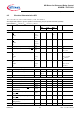
SO
SCLK
SI
CS
GND
IN
VDD
RST
VDDA
Application .emf
OUT0
OUT1
OUT2
OUT3
Vbb
Loads
Vdda
SPI uC
PWM
Vdd
C1
C2
C3
R2
R3
R5
R6
R4
R1
TLE 7231G