
Datasheet

Datasheet 27 Rev. 1.1, 2011-04-12
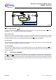
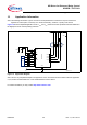
SPI Driver for Enhanced Relay Control
SPIDER - TLE7231G
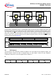
Serial Peripheral Interface (SPI)
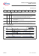
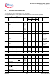
9.5 Electrical Characteristics SPI
V
DD
= 3.0 V to V
DDA
, V
DDA
= 4.5V to 5.5V, T
j
= -40 °C to +150 °C
All voltages with respect to ground, positive current flowing into pin (unless otherwise specified)
typical values:
V
DD
= 5.0 V, V
DDA
= 5.0 V, T
j
= 25 °C
Pos. Parameter Symbol Limit Values Unit Conditions
Min. Typ. Max.
Input Characteristics (CS
, SCLK, SI)
9.5.1 L level of pin
CS
SCLK
SI
V
CS(L)
V
SCLK(L)
V
SI(L)
0 – 0.2*
V
DD
–
9.5.2 H level of pin
CS
SCLK
SI
V
CS(H)
V
SCLK(H)
V
SI(H)
0.5*V
DD
– V
DD
–
9.5.3 L-input pull-up current through CS
I
CS(L)
51740µA V
CS
= 0 V
9.5.4 H-input pull-up current through CS
I
CS(H)
31540µA
1)
V
CS
= 2 V
9.5.5 L-input pull-down current through
pin
SCLK
SI
I
SCLK(L)
I
SI(L)
31280µA
1)
V
SCLK
= 0.6 V
V
SI
= 0.6 V
9.5.6 H-input pull-down current through
pin
SCLK
SI
I
SCLK(H)
I
SI(H)
10 40 80 µA
V
SCLK
= 5 V
V
SI
= 5 V
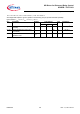
Output Characteristics (SO)
9.5.7 L level output voltage
V
SO(L)
0–0.4VI
SO
= -2 mA
9.5.8 H level output voltage
V
SO(H)
V
DD
-
0.5 V
– V
DD
I
SO
= 1.5 mA
9.5.9 Output tristate leakage current
I
SO(OFF)
-10 – 10 µA V
CS
= V
DD
Timings
9.5.10 Serial clock frequency
f
SCLK
0 –5MHz–
9.5.11 Serial clock period
t
SCLK(P)
200––ns–
9.5.12 Serial clock high time
t
SCLK(H)
50––ns–
9.5.13 Serial clock low time
t
SCLK(L)
50––ns–
9.5.14 Enable lead time (falling CS
to
rising SCLK)
t
CS(lead)
250––ns–
9.5.15 Enable lag time (falling SCLK to
rising CS
)
t
CS(lag)
250––ns–
9.5.16 Transfer delay time (rising CS
to
falling CS
)
t
CS(td)
250––ns–
9.5.17 Data setup time (required time SI to
falling SCLK)
t
SI(su)
20––ns–
9.5.18 Data hold time (falling SCLK to SI)
t
SI(h)
20––ns–