
Datasheet

Datasheet 23 Rev. 1.1, 2011-04-12
SPI Driver for Enhanced Relay Control
SPIDER - TLE7231G
Serial Peripheral Interface (SPI)
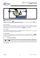
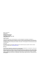
Figure 11 Transmission Error Flag on SO Line
CS
Low to High transition:
Data from shift register is transferred into the input matrix register only, when after the falling edge of CS
exactly
a multiple (1, 2, 3, …) of eight SCLK signals have been detected.
SCLK - Serial Clock:
This input pin clocks the internal shift register. The serial input (SI) transfers data into the shift register on the falling
edge of SCLK while the serial output (SO) shifts diagnostic information out on the rising edge of the serial clock.
It is essential that the SCLK pin is in low state whenever chip select CS
makes any transition.
SI - Serial Input:
Serial input data bits are shifted in at this pin, the most significant bit first. SI information is read on the falling edge
of SCLK. Please refer to Section 9.3 for further information.
SO - Serial Output:
Data is shifted out serially at this pin, the most significant bit first. SO is in high impedance state until the CS
pin
goes to low state. New data will appear at the SO pin following the rising edge of SCLK. Please refer to Section 9.3
for further information.
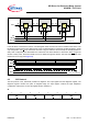
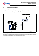
9.2 Daisy Chain Capability
The SPI of TLE7231G provides daisy chain capability. In this configuration several devices are activated by the
same CS
signal MCS. The SI line of one device is connected with the SO line of another device (see Figure 12),
which builds a chain. The ends of the chain are connected with the output and input of the master device, MO and
MI respectively. The master device provides the master clock MCLK, which is connected to the SCLK line of each
device in the chain.
TE R. emf
SI
SPI
OR
TER
0
1
SO
CS
SCLK
S
SO
S
SI