
Datasheet

Datasheet 15 Rev. 1.1, 2011-04-12
SPI Driver for Enhanced Relay Control
SPIDER - TLE7231G
Power Stages
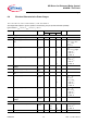
6.4.13 Output leakage current
(per channel)
I
D(OFF)
––
1
2
5
µA
V
DS
= 13.5 V
T
j
= 25 °C
1)
T
j
= 85 °C
1)
T
j
= 150 °C
6.4.14 Output clamping voltage
V
DS(CL)
41 – 52 V
3)
Input Pin Characteristics
6.4.15 L level of pin IN
V
IN(L)
0–0.9V–
6.4.16 H level of pin IN
V
IN(H)
2.2 – 5.5 V –
6.4.17 L-input pull-down current through
pin
I
IN(L)
31280µA V
DD
= 5 V
1)
V
IN
= 0.6 V
6.4.18 H-input pull-down current through
pin
I
IN(H)
10 40 80 µA V
DD
= 5 V
V
IN
= 5 V
6.4.19 L level of pin RST
V
RST(L)
0 – 0.2*
V
DD
–
6.4.20 H level of pin RST
V
RST(H)
0.4*
V
DD
– V
DD
–
6.4.21 L-input pull-down current through
pin RST
I
RST(L)
31280µA V
DD
= 5 V
1)
V
RST
= 0.6 V
6.4.22 H-input pull-down current through
pin RST
I
RST(H)
10 40 80 µA V
DD
= 5 V
V
RST
= 5 V
Timings
6.4.23 Sleep wake-up time
t
wu(sleep)
––200µs–
6.4.24 Reset duration
t
RST(L)
1––µs–
6.4.25 Turn-on time
V
DS
= 20% V
bat
t
ON
––60µs V
bb
= 13.5 V
I
DS
= 250 mA,
resistive load
6.4.26 Turn-off time
V
DS
= 80% V
bb
t
OFF
––60µs V
bb
= 13.5 V
I
DS
= 250 mA,
resistive load
1) Not subject to production test, specified by design
2)
calculated value based on following parameters:
all channels on with equal load current, R
DS(ON)
= R
DS(ON,150°C)
, T
a
= 85 °C, T
j,max
= 150 °C, R
th
= R
thJA(typ)
3) maximum value is increasing in sleep mode
V
DD
= 3.0 V to V
DDA
, V
DDA
= 4.5V to 5.5V, T
j
= -40 °C to +150 °C
All voltages with respect to ground, positive current flowing into pin (unless otherwise specified)
typical values:
V
DD
= 5.0 V, V
DDA
= 5.0 V, T
j
= 25 °C
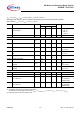
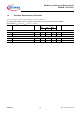
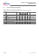
Pos. Parameter Symbol Limit Values Unit Conditions
Min. Typ. Max.