
Datasheet

Datasheet 13 Rev. 1.1, 2011-04-12
SPI Driver for Enhanced Relay Control
SPIDER - TLE7231G
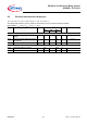
Power Stages
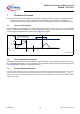
Figure 5 Output Clamp Implementation
Maximum Load Inductance
During demagnetization of inductive loads, energy has to be dissipated in the TLE7231G.
This energy can be calculated with following equation:
Following equation simplifies under the assumption of
R
L
= 0:
The maximum energy, which is converted into heat, is limited by the thermal design of the component.
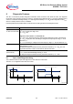
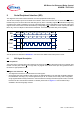
6.3 Timing Diagrams
The power transistors are switched on and off with a dedicated slope via the IN bits of the serial peripheral
interface SPI. The switching times
t
ON
and t
OFF
are designed equally.
Figure 6 Switching a Resistive Load
In input mode, a high signal at the input pin is equivalent to a SPI ON command and a low signal to SPI OFF
command respectively. Please refer to Section 9.3 for details on operation modes.
The listed switching times are not valid, when switching to or from stand-by mode.
OutputClamp .emf
V
bat
I
D
V
DS( CL )
OUT
V
DS
GND
L,
R
L
EV
DS(CL)
V
bat
V–
DS(CL)
R
L
------------------------------------
ln⋅ 1
R
L
I
L
⋅
V
bat
V–
DS(CL)
------------------------------------–
I
L
+
L
R
L
------
⋅⋅=
E
1
2
---
LI
L
2
1
V
bat
V
bat
V–
DS(CL)
------------------------------------–
⋅=
CS
V
DS
t
SwitchOn.emf
t
ON
t
OFF
t
20%
80%
SPI: ON SPI: OFF