
Datasheet

Data Sheet 9 V2.1, 2008-04-30
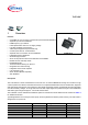
TLE7183F
General Product Characteristics
Attention: Stresses above the ones listed here may cause permanent damage to the device. Exposure to
absolute maximum rating conditions for extended periods may affect device reliability.
Attention: Integrated protection functions are designed to prevent IC destruction under fault conditions
described in the data sheet. Fault conditions are considered as “outside” normal operating
range. Protection functions are not designed for continuous repetitive operation.
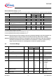
4.2 Functional Range
4.1.28 Peak reflow soldering temperature
2)
T
ref
–260°C–
Thermal Resistance
4.1.29 Junction to case
R
thjC
–5K/W–
Power Dissipation
4.1.30 Power Dissipation (DC) @
TCASE=125°C
P
tot
–2W–
ESD Susceptibility
4.1.31 ESD Resistivity
3)
V
ESD
–2kV
4.1.32 ESD Resistivity (charge device model)
4)
V
ESD
–750V
1) Not subject to production test, specified by design.
2) Reflow profile IPC/JEDEC J-STD-020C
3) ESD susceptibility HBM according to EIA/JESD 22-A 114B
4) ESD susceptibility CDM according to EIA/JESD 22-C 101
Pos. Parameter Symbol Limit Values Unit Conditions
Min. Max.
4.2.1 Supply voltage
1)2)
V
S
5.5
5.5
20
28
VDC
t<1s
4.2.2 Duty cycle
3)
D 0 100 % –
4.2.3 PWM frequency
F
PWM
0 25 kHz Total gate charge
400nC
4.2.4 Quiescent current
4)
I
Q
–30µAV
S
,V
DH
<20 V
4.2.5 Quiescent current into VDH
I
Q_VDH
–30µAV
DH
<20V;
V
S
pin open
4.2.6 Supply current at Vs
I
Vs
–
–
175
175
110
110
mA
F
PWM
=25kHz
Q
G
=250nC:
V
S
= 5.5V
V
S
= 14V
V
S
= 17V
V
S
= 20V
4.2.7 Supply current at Vs(device
disabled by ENA)
I
Vs(o)
–60
50
mA Vs=5.5V..17V
Vs=17V..20V
4.2.8 Currrent into VDH (device not in
sleep mode)
I
VDH
1.5 mA V
VDH
=5.5..20V
INH=high
Absolute Maximum Ratings (cont’d)
1)
40 °C ≤ T
j
≤ 150 °C; all voltages with respect to ground, positive current flowing into pin (unless otherwise specified)
Pos. Parameter Symbol Limit Values Unit Conditions
Min. Max.