
Datasheet

TLE7183F
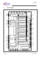
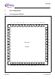
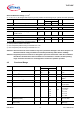
Pin Configuration
Data Sheet 6 V2.1, 2008-04-30
3.2 Pin Definitions and Functions
Pin Symbol Function
1 SL3 Connection to source low side switch 3
2 GND Logic and power ground
3 VO Output of OpAmp for shunt signal amplification
4 ISN - Input of OpAmp for shunt signal amplification
5 ISP + Input of OpAmp for shunt signal amplification
6 VRI Input of bias reference amplifier
7 VRO Output of bias reference amplifier
8 AGND Analog ground especially for the current sense OpAmp
9 VTHOC Threshold voltage for overcurrent detection
10 TP test pin, connect to GND of driver IC
11 DT Dead time program pin
12 INH Inhibit pin (active low)
13 IL3 Input for low side switch 3 (active high)
14 IH3 Input for high side switch 3 (active low)
15 U_fb Digital logic representation of the voltage phase U; positive logic
16 V_fb Digital logic representation of the voltage phase V; positive logic
17 W_fb Digital logic representation of the voltage phase W; positive logic
18 ENA1 Enable pin (active high)
19 ENA2 Enable pin (active high)
20 GND Logic and power ground
21 IL1 Input for low side switch 1 (active high)
22 IH1 Input for high side switch 1 (active low)
23 IL2 Input for low side switch 2 (active high)
24 IH2 Input for high side switch 2 (active low)
25 ERR1 Error signal 1
26 ERR2 Error signal 2
27 CH2 + terminal for pump capacitor of charge pump 2
28 CH1 + terminal for pump capacitor of charge pump 1
29 CL1 - terminal for pump capacitor of charge pump 1
30 VS Voltage supply
31 CL2 - terminal for pump capacitor of charge pump 2
32 GND Logic and power ground
33 CB1 Buffer capacitor for charge pump 1
34 VDH Connection to drain of high side switches for short circuit detection
35 GL1 Output to gate low side switch 1
36 SL1 Connection to source low side switch 1
37 GND Logic and power ground
38 SH1 Connection to source high side switch 1
39 GH1 Output to gate high side switch 1
40 CB2 Buffer capacitor for charge pump 2